Area cost — wide muxes, case bloat, resource sharing
Every line of RTL becomes gates on silicon. Area drives cost, power, and routability. RTL authors control area through mux width, duplicated vs shared arithmetic, and the choice between random logic and memories.
A 2:1 mux on W bits ≈ W transmission gates. A 32-bit adder ≈ hundreds of gates. A 256×32 ROM may be smaller than the same table built from case statements — synthesis decides, but your RTL shapes the outcome.
Wide muxes — the silent area tax
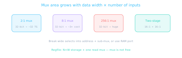
Forwarding muxes in CPUs are wide and numerous — area budgeted explicitly. Don't duplicate blindly in small blocks either.
A mux with N inputs of width W scales roughly as O(N × W) transmission gates. A 256:1 mux on a 32-bit bus is not "just a case statement" — it is a physical monster that also hurts timing (Lesson 9.9).
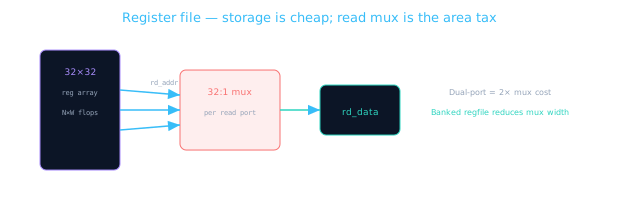
Every read port adds a wide mux. Module 6 regfile lessons — same area intuition applies at signoff.
| RTL pattern | Area driver | Mitigation |
|---|---|---|
case(sel) 256 items | Large mux or LUT tree | ROM/sync RAM inference; two-level decode |
| Per-channel duplicate ALU | N × ALU area | Shared ALU + time-multiplex (resource sharing) |
| 128-bit internal buses | Wide wire + mux everywhere | Narrow to where needed; pack fields |
| Parallel CRC lanes | 4× polynomial logic | One lane, 4 cycles if throughput allows |
Case statement bloat vs ROM inference
// 256-entry lookup — may infer huge combo logic
always @(*) begin
  case (addr[7:0])
    8'h00: lut_out = 32'hDEAD0000;
    8'h01: lut_out = 32'hDEAD0001;
    // ... 254 more rows — maintenance nightmare + area risk
    8'hFF: lut_out = 32'hDEAD00FF;
  endcase
end
// Synthesis-friendly: explicit ROM / sync RAM inference
reg [31:0] rom [0:255];
initial begin
  for (int i = 0; i < 256; i++)
    rom[i] = 32'hDEAD0000 + i;  // or $readmemh for real coeffs
end

always @(posedge clk)
  lut_out <= rom[addr[7:0]];  // 1-cycle latency, compact memory
When logic beats ROM: Sparse functions, runtime-programmable tables, or tiny (<16 entry) decodes where a mux is genuinely smaller. Always check the area report — don't assume.
// 256:1 via 16:1 + 16:1 — shallower tree, often better timing too
wire [3:0] bank = addr[7:4];
wire [3:0] idx   = addr[3:0];
wire [31:0] bank_out [0:15];

genvar g;
generate for (g = 0; g < 16; g = g + 1) begin : banks
  assign bank_out[g] = lut_bank[g][idx];  // 16-entry sub-tables
end endgenerate

assign lut_out = bank_out[bank];  // final 16:1 mux — not 256:1
Resource sharing — one ALU, many clients
When operations are mutually exclusive in time, share hardware instead of instantiating duplicates.
// 3 parallel ALUs — 3× area if only one runs per cycle
wire [31:0] add_result = a + b;
wire [31:0] sub_result = c - d;
wire [31:0] and_result = e & f;
assign out = sel[0] ? add_result : sel[1] ? sub_result : and_result;
// Shared ALU — mux operands in, demux result out
reg [1:0] op_q;
reg [31:0] a_q, b_q;

wire [31:0] alu_out = (op_q == OP_ADD) ? a_q + b_q :
                      (op_q == OP_SUB) ? a_q - b_q :
                                         a_q & b_q;

always @(posedge clk) begin
  if (issue) begin op_q <= op; a_q <= a_in; b_q <= b_in; end
  result <= alu_out;  // +1 cycle latency — document in spec
end
Sharing without a scheduler causes structural hazards (Lesson 8.2). If two clients need the ALU same cycle, you must stall or duplicate. Area saved ≠ free throughput.
// Shared ALU with explicit grant — avoids structural hazard
reg alu_busy;
wire grant_a = req_a && !alu_busy;
wire grant_b = req_b && !alu_busy && !req_a;  // priority to A

always @(posedge clk) begin
  if (grant_a || grant_b) begin
    alu_busy <= 1'b1;
    op_q  <= grant_a ? op_a : op_b;
    a_q   <= grant_a ? a_a  : a_b;
    b_q   <= grant_a ? b_a  : b_b;
  end else
    alu_busy <= 1'b0;
end
// Stall clients without grant — document +1 cycle minimum latency
Memory vs random logic — the inference decision
Synthesis maps large tables to SRAM macros or register files when the access pattern is regular. Irregular sparse logic may stay as LUT clouds — expensive.
| Pattern | Likely inference | Area intuition |
|---|---|---|
reg [W-1:0] mem [0:N] + posedge read | Sync SRAM / register file | Compact for N > 32 |
case(addr) with 512 rows | Giant mux or LUT | Often 3–10× larger than RAM |
| Distributed RAM (Xilinx) / LC (Intel) | Small shallow memories | Good for N < 64, shallow |
| Single-port vs dual-port | 2× read bandwidth | 2× memory area + muxes |
// Production pattern: coeffs live in .mem file, infer ROM at synth
reg [15:0] coeffs [0:255];
initial $readmemh("fir_coeffs.hex", coeffs);

always @(posedge clk)
  coeff_out <= coeffs[tap_idx];  // tool infers ROM block
FPGA vs ASIC: FPGAs have fixed BRAM tiles — odd widths (e.g. 18×512) may waste tiles. ASIC SRAM compilers are flexible but have minimum area. Read the technology guide before picking width/depth.
Pipeline adds flops, removes combo — area trade
Pipelining (Module 8) trades flop area for shorter combo clouds. A 32-bit multiplier in one cycle may need a huge Booth array; a 3-stage pipe uses less combo area per stage but adds 64+ flop bits per stage.
More pipeline stages
More flops (area ↑), less combo per stage (timing ↑), latency ↑.
Fewer stages
Less flop area, deeper combo (timing ↓), lower latency.
Sweet spot
Enough stages to meet Fmax with positive slack — no more.
# Synthesis area report — fields RTL authors actually read
Cell Count:     12450   (total instances)
Flop Count:      3200   (register bits / 1 — watch growth from pipelining)
Memory Count:       2   (inferred ROM/RAM — good if you expected tables)
Combinational:   8450   (mux + arithmetic — watch case bloat)

# Compare before/after RTL change — trend matters more than absolute
Area review checklist
- Check synthesis area report after major RTL changes — trend matters
- Question every wide mux: can select be narrower or registered?
- Large case/LUT tables → try ROM/RAM inference with
$readmemh - Mutually exclusive ops → consider shared ALU/multiplier
- Balance area vs timing: pipelining adds flops (area) but saves combo (timing)
- Don't micro-optimize until block is functionally correct — but don't ignore 10× bloat
🎯 What to remember
- Wide muxes scale with width × inputs — major hidden area cost.
- Case bloat on large tables → prefer ROM/RAM inference.
- Resource sharing saves area when ops don't overlap in time.
- Area, timing, and power trade off — document latency when sharing.