Mini case study: one feature followed Spec → PD
Let’s glue Module 1 together with a single story: adding an I2C master to a small SoC. You will meet this feature again as the course capstone — for now, watch how every stage touches it.
Spec
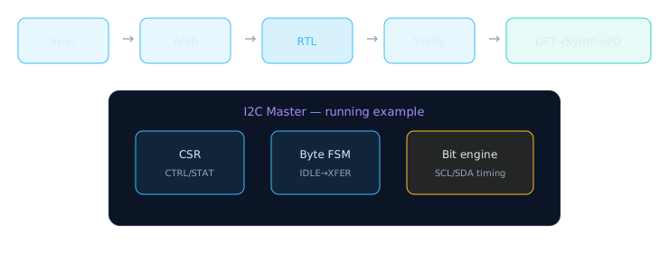
One feature, every stage — Module 11 builds this for real.
- MUST support standard-mode I2C master writes/reads
- MUST expose status (BUSY, NACK) to software via CSR
- SHOULD support clock stretching
- Acceptance: directed TB proves START → address → data → STOP
Spec detail — who owns what
| Artifact | Owner | Skip risk |
|---|---|---|
| I2C timing MUST lines | Systems + RTL lead | Bus violations, sensor reads fail |
| CSR register ABI | Architect + firmware | Driver rewrites every week |
| Acceptance tests A1–A4 | DV + designer | “Works in sim once” ships |
MUST M6: On ABORT during BUSY, release SCL/SDA to idle within 1 byte time
MUST M7: STAT.NACK sticky until software write-1-to-clear

ACCEPTANCE A5: Write 0x3A, slave NACK → STAT.NACK=1, BUSY=0, SDA released
Architecture
Blocks: CSR bank, byte FSM, bit engine (SCL/SDA timing), APB/AXI-lite slave port, interrupt line.
Clocks: system clock domain for CSR/FSM; note open-drain pad domain considerations.
Draw CDC if any async inputs exist (e.g. external stretch events sampled carefully).
SoC narrative: CPU writes CSR to kick a transfer. Byte FSM sequences address + data bytes. Bit engine toggles SCL and samples SDA at the right micro-delays. IRQ fires on DONE so firmware does not poll forever. PD places I2C near pad ring; STA checks paths from FSM flops to SCL output buffer.
One engineer codes “everything in one module” — reviews take days, unit tests impossible, PD cannot pipeline pad path.
RTL design
Implement synthesizable Verilog for bit/byte engines + registers. Keep outputs registered where helpful.
Practice later in Modules 3–7; prove ideas in the simulator.
CSR map sketch + a tiny FSM skeleton (you will expand this in the capstone):
Offset  Name     Bits
0x00    CTRL     [0]=START  [1]=ABORT  [2]=IRQ_EN
0x04    STAT     [0]=BUSY   [1]=NACK   [2]=DONE  (sticky NACK)
0x08    ADDR     [6:0]=7-bit slave address  [7]=R/W
0x0C    TXDATA   [7:0]=byte to write
0x10    RXDATA   [7:0]=byte read from bus
// Skeleton only — full I2C comes in Module 11
module i2c_byte_fsm (
  input  wire clk,
  input  wire rst_n,
  input  wire start_cmd,
  input  wire bit_done,
  input  wire nack,
  output reg  busy
);
  localparam IDLE = 2'd0, XFER = 2'd1, DONE = 2'd2;
  reg [1:0] state, next;

  always @(posedge clk or negedge rst_n) begin
    if (!rst_n) state <= IDLE;
    else        state <= next;
  end

  always @(*) begin
    next = state;
    busy = 1'b0;
    case (state)
      IDLE: if (start_cmd) next = XFER;
      XFER: begin
        busy = 1'b1;
        if (bit_done && nack) next = DONE;
        else if (bit_done)    next = DONE; // simplify for sketch
      end
      DONE: next = IDLE;
      default: next = IDLE;
    endcase
  end
endmodule
▶ Experiment with the FSM skeleton
CSR expanded — software contract
CTRL [0] START   — write 1 to begin (self-clear or pulse)
CTRL [1] ABORT   — force bus recovery
CTRL [2] IRQ_EN  — mask DONE interrupt
STAT [0] BUSY    — read-only, 1 during transfer
STAT [1] NACK    — sticky, W1C (write 1 to clear)
STAT [2] DONE    — sticky, W1C
PRESCALE — divider for SCL from clk_sys
Firmware polls wrong bits; “driver bug” debates hide missing sticky NACK spec.
Verification
- Reset clears BUSY
- Write transaction ACKs
- NACK path sets sticky status
- Back-to-back transfers don’t hang
Verification plan bullets
- Smoke: reset, single byte write, wave review
- Directed: A1–A5 from spec (ACK, NACK, abort, stretch)
- Corner: START during BUSY (illegal — must ignore or error)
- Regression: run on every RTL commit
- Coverage goal: all FSM states + NACK + DONE IRQ path
TEST smoke_reset:     rst_n low → BUSY=0, STAT=0
TEST directed_write:  START, addr 0x50, data 0xAB, STOP, expect ACK
TEST nack_addr:       slave NACK on addr → STAT.NACK=1
TEST abort_mid:       ABORT during byte 3 → bus idle, BUSY=0
Silicon returns from fab; first board test finds NACK never clears — 8-week debug while competitors ship.
DFT / Synthesis / PD / Sign-off (awareness)
- DFT — scan-friendly flops; don’t break test modes around pads.
- Synthesis — constraints include I2C clocking relationships / IO delays.
- PD — place near appropriate IO; watch congestion on bus fabrics.
- Sign-off — STA on paths to pads; DRC around ESD/IO cells (team specialty).
Spec is the script. Architecture is storyboarding. RTL is filming scenes. Verification is editing. DFT/PD/sign-off are VFX + theatrical release checks. Skipping early stages makes the premiere a disaster.
What goes wrong if a stage is skipped
| Skipped stage | I2C-specific failure |
|---|---|
| Spec | No abort behavior — hung bus needs chip reset |
| Arch | Bit timing mixed into CSR — unmaintainable |
| RTL | Nothing to integrate |
| Verify | NACK corner ships broken |
| DFT | Low scan coverage — factory scrap |
| Synth | No timed netlist for PD |
| PD | Pad path fails setup — slow or dead I2C |
| Sign-off | Foundry reject or field failures |
“Tell me about a block you designed” — Use I2C: spec MUST lines → arch blocks → FSM states → tests run → how PD/sign-off would touch pad timing.
Your Module 1 checkpoint
You should now be able to explain, in order, what happens to a feature from idea to tape-out — and where RTL sits.
- Name each major stage in the VLSI flow
- Explain why verification and DFT are not “someone else’s problem only”
- Describe how RTL style affects synthesis and PD
Next module: Digital Foundations — bits, clocks, reset, and waveform literacy before deep Verilog.
🎯 What to remember
- One feature touches Spec → Arch → RTL → Verify → DFT → Synth → PD → Sign-off.
- I2C is our running example and future capstone.
- Module 1 complete: you have the map of the chip world.
- Continue from the course index into Module 2 when published.