Architecture — blocks, interfaces, clocks, power domains
Architecture is the map of the city before drawing every house. You decide the blocks, how they talk, which clocks they use, and which power islands exist — so RTL does not invent chaos later.
Blocks and hierarchy
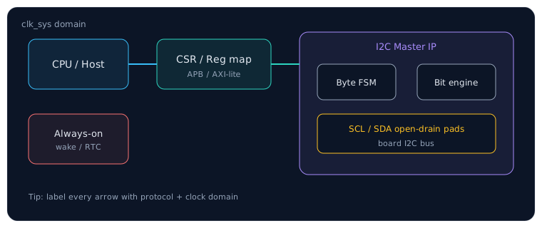
Architecture deliverable: blocks, named interfaces, clocks, and power islands on one page.
Good architectures split by responsibility:
- Datapath — compute / move data
- Control — FSMs that sequence the datapath
- Interfaces — I2C, UART, AXI, memory ports
- CSR / register map — software-visible knobs
Rule of thumb: if two teams can argue about ownership of a signal, draw a block boundary and name the interface.
Hierarchy decisions — when to split blocks
| Split when… | Keep together when… |
|---|---|
| Different owners or reuse (I2C IP in many chips) | Tight feedback loop (< 5 cycles) and one reviewer |
| Clear protocol boundary (CSR vs bit engine) | Splitting adds latency you cannot afford |
| PD needs a register slice between regions | Block is tiny (< 500 lines) and stable |
| Verification can unit-test in isolation | Interface would be wider than the logic inside |
Our I2C master splits into CSR (software contract), byte FSM (transaction sequencing), and bit engine (line timing) — three reviewable pieces.
Architects draw boxes so RTL leads can parallelize. If your diagram has one giant “logic” blob, schedule risk is hidden until week 20.
Interfaces beat spaghetti
Prefer clear protocols (valid/ready, req/ack, AXI-lite, I2C open-drain) over anonymous wires named flag3.
Named ports
Document width, direction, reset value, and clock domain on the diagram.
Skid / FIFO
Decouple producers and consumers so timing and rate differ safely.
Valid/ready handshake — the most common on-chip streaming interface:
// Transfer occurs when BOTH are high (same cycle)
// valid: source has data
// ready: sink can accept
//
//   valid __|‾‾|________|‾‾|
//   ready ______|‾‾|________|‾‾|
//   data  ----<D0>--------<D1>----
//
// Rule: once valid=1, data must stay stable until handshake (ready=1)

module valid_ready_sink (
  input  wire       clk,
  input  wire       valid,
  output reg        ready,
  input  wire [7:0] data
);
  // Architecture doc should say: clk_sys domain, no back-pressure on I2C CSR path
endmodule
Mixing req/ack and valid/ready on the same bus without documenting semantics — DV will write tests for the wrong protocol.
Clocks (where CDC begins)
Every flop lives in a clock domain. Crossing domains without a plan is a future silicon bug.
- List every clock and its source (PLL, pad, divided).
- Mark which blocks sit in which domain.
- If a signal crosses domains, name the synchronizer strategy (Module 9 + CDC course).
Beginner trap: “We’ll just sample it; it’s slow.” Slow multi-bit buses still tear. Architecture must admit CDC early.
Clock domain documentation template
Clock      Source      Frequency   Blocks in domain
clk_sys    PLL div2    50 MHz      CPU, CSR, I2C FSM, bit engine
clk_aon    XTAL        32 kHz      RTC, wake timer
pad_async  external    async       SCL/SDA inputs (sample in clk_sys)

CDC crossings:
  C1: stretch_detect (pad_async → clk_sys) — 2-flop sync, single-bit
  C2: (none) CSR and FSM share clk_sys — no CDC between them
Power domains (awareness level)
Modern chips shut islands off. Architecture notes:
- Which blocks can power-gate?
- What must stay always-on (wake logic, RTC)?
- Isolation / retention needs (you’ll meet these words again in DFT/PD).
You do not need UPF mastery yet — you need to not be surprised when power shows up in reviews.
Floorplan-aware architecture
PD teams place IO macros near package pins. If I2C talks to board sensors, architect the master near the I2C pad ring — not on the opposite corner from the CPU with a 5 mm wide CSR bus snaking across the die.
- Keep high-toggle buses local or pipelined.
- Separate always-on wake logic from power-gated compute.
- Note which blocks need retention flops when power-gated.
Architecture anti-patterns
| Anti-pattern | Why it hurts | Better |
|---|---|---|
| “Global state” wire fanout | Timing + verification explosion | CSR + explicit handshakes |
| Undocumented CDC | Metastability, random bugs | CDC table + synchronizer per crossing |
| One mega-FSM | Unreviewable, untestable | Layer FSMs (byte + bit) |
| Ad-hoc scratch registers | Software ABI chaos | Versioned register map doc |
“Walk me through your block diagram” — practice narrating data flow, clocks, and one CDC point in under 90 seconds.
Deliverable of architecture
- One block diagram with clocks labeled
- Interface list (widths + protocol)
- Known CDC points
- Register map outline (even a stub)
Even before full RTL, architects sketch the top-level ports — this is the “contract” between blocks:
module i2c_master (
  // Clock / reset (clk_sys domain)
  input  wire        clk,
  input  wire        rst_n,

  // CSR / host bus (simplified)
  input  wire        csr_we,
  input  wire [7:0]  csr_addr,
  input  wire [31:0] csr_wdata,
  output reg  [31:0] csr_rdata,
  output wire        irq,

  // I2C pads (open-drain style)
  inout  wire        scl,
  inout  wire        sda
);
  // Architecture note:
  // - Byte FSM + bit engine live here
  // - Document any CDC if pads/events are async
endmodule
SoC diagram narrative — read the arrows
Follow one write transaction through the diagram above:
- CPU issues APB write to CSR CTRL.START
- CSR block pulses
start_cmdto byte FSM (same clock domain) - Byte FSM requests bit periods from bit engine
- Bit engine drives SCL/SDA pads (open-drain, timing-critical)
- On DONE, CSR sets STAT and optionally asserts IRQ to CPU
Every arrow should have a label: signal name, width, protocol, clock domain. If it does not fit on the diagram, the architecture is not finished.
🎯 What to remember
- Architecture decides blocks, interfaces, clocks, and power before RTL details.
- Named protocols beat mystery wires.
- CDC and power must be drawn, not discovered accidentally.
- Next: what RTL designers actually do day to day.