Lab: programmable datapath slice
Wire Module 7 into one block. You build prog_datapath — a 4-register file, muxed ALU, and 5-state control FSM that executes 8-bit instructions with opcode, source registers, and destination. This is the Module 7 checkpoint.
Produce a synthesizable prog_datapath module plus self-checking testbench you can paste into the EcrioniX Verilog simulator. Demonstrates skid-buffer thinking, memory/regfile access, and control/datapath co-design.
Instruction format & ISA
| Bits | Field | Description |
|---|---|---|
[7:6] | opcode | 00=ADD, 01=SUB, 10=AND, 11=XOR |
[5:4] | rs | Source register A (r0–r3) |
[3:2] | rt | Source register B (r0–r3) |
[1:0] | rd | Destination register (r0–r3) |
Semantics: rd = rs OP rt (e.g. ADD r1,r2,r3 → r3 = r1 + r2).
This is a tiny CPU with one instruction and four variables. The control FSM is the "execute" button — press start, feed an instruction, wait for done, read the result from the regfile.
Block diagram
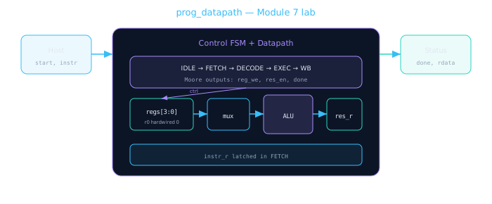
One instruction per start pulse. Result visible on rdata when done asserts.
Interface spec
- Inputs:
clk,rst_n,start(pulse to begin),instr[7:0] - Outputs:
done(high in WB),rdata[7:0](readback of dest reg after write) - Convention:
regs[0] = 0always (writes to r0 ignored) - Style: 3-block Moore FSM, safe
default → IDLE
Control micro-op table
| State | reg_we | res_en | done | Action |
|---|---|---|---|---|
IDLE | 0 | 0 | 0 | Wait for start |
FETCH | 0 | 0 | 0 | Latch instr → instr_r |
DECODE | 0 | 0 | 0 | Parse fields (combo) |
EXEC | 0 | 1 | 0 | ALU compute → result_r |
WB | 1 | 0 | 1 | Write result_r → regs[rd] |
Writing regs[rd] <= alu_out in EXEC bypasses result_r and can glitch if ALU inputs change. Always register the ALU output before writeback.
Full DUT — paste-ready module
// prog_datapath — Module 7.5 lab DUT
// 4-reg programmable ALU slice with 5-state control FSM
module prog_datapath (
  input  wire       clk,
  input  wire       rst_n,
  input  wire       start,
  input  wire [7:0] instr,
  output wire       done,
  output wire [7:0] rdata
);
  localparam IDLE=0, FETCH=1, DECODE=2, EXEC=3, WB=4;

  reg [2:0] state, next;
  reg [7:0] instr_r;
  reg [7:0] regs [0:3];
  reg [7:0] result_r;

  wire [1:0] rs  = instr_r[5:4];
  wire [1:0] rt  = instr_r[3:2];
  wire [1:0] rd  = instr_r[1:0];
  wire [1:0] op  = instr_r[7:6];

  wire [7:0] op_a = regs[rs];
  wire [7:0] op_b = regs[rt];
  wire [7:0] alu_out =
    (op == 2'b00) ? op_a + op_b :
    (op == 2'b01) ? op_a - op_b :
    (op == 2'b10) ? op_a & op_b :
                     op_a ^ op_b;

  wire reg_we = (state == WB);
  wire res_en = (state == EXEC);
  assign done  = (state == WB);
  assign rdata = regs[rd];

  // Block 1: state + datapath registers
  always @(posedge clk or negedge rst_n) begin
    if (!rst_n) begin
      state    <= IDLE;
      instr_r  <= 8'h00;
      result_r <= 8'h00;
      regs[0]  <= 8'h00;
      regs[1]  <= 8'h00;
      regs[2]  <= 8'h00;
      regs[3]  <= 8'h00;
    end else begin
      state <= next;
      if (state == FETCH)  instr_r  <= instr;
      if (res_en)          result_r <= alu_out;
      if (reg_we && rd != 2'b00) regs[rd] <= result_r;
      regs[0] <= 8'h00;  // r0 hardwired zero
    end
  end

  // Block 2: next-state
  always @(*) begin
    next = IDLE;
    case (state)
      IDLE:   if (start) next = FETCH;
      FETCH:  next = DECODE;
      DECODE: next = EXEC;
      EXEC:   next = WB;
      WB:     next = IDLE;
      default: next = IDLE;
    endcase
  end
endmodule
Self-checking testbench
module prog_datapath_tb;
  reg clk, rst_n, start;
  reg [7:0] instr;
  wire done;
  wire [7:0] rdata;

  prog_datapath dut (
    .clk(clk), .rst_n(rst_n),
    .start(start), .instr(instr),
    .done(done), .rdata(rdata)
  );

  initial clk = 0;
  always #5 clk = ~clk;

  integer errors;
  task run_insn(input [7:0] ins, input [7:0] expect);
    begin
      @(posedge clk); start = 1; instr = ins;
      @(posedge clk); start = 0;
      wait(done);
      @(posedge clk);
      if (rdata !== expect) begin
        $display("FAIL: insn=%h got %h expected %h", ins, rdata, expect);
        errors = errors + 1;
      end else
        $display("PASS: insn=%h result=%h", ins, rdata);
    end
  endtask

  initial begin
    errors = 0;
    rst_n = 0; start = 0; instr = 0;
    #20 rst_n = 1;

    // Preload r1=10, r2=4 via backdoor (sim only)
    dut.regs[1] = 8'd10;
    dut.regs[2] = 8'd4;

    // ADD r1,r2,r3 → expect 14
    run_insn(8'b00011011, 8'd14);

    // SUB r1,r2,r3 → expect 6
    run_insn(8'b01011011, 8'd6);

    // AND r1,r2,r3 → expect 10 & 4 = 0
    run_insn(8'b10011011, 8'd0);

    // XOR r1,r2,r3 → expect 10 ^ 4 = 14
    run_insn(8'b11011011, 8'd14);

    // Write to r0 should be ignored (stay 0)
    dut.regs[3] = 8'hFF;
    run_insn(8'b00011000, 8'd0);  // ADD r1,r2,r0

    if (errors == 0) $display("=== ALL TESTS PASSED ===");
    else $display("=== %0d TESTS FAILED ===", errors);
    $finish;
  end
endmodule
Extension challenges
Add LOAD/STORE
Extend opcode space: load immediate into reg, or read from a small sync FIFO input port.
Skid on input
Wrap the instruction port with a skid buffer so back-to-back start pulses work without waiting for done.
Pipeline to 2-cycle
Split EXEC into EXE1 (operand read) and EXE2 (ALU) — update micro-op table accordingly.
Module 7 checkpoint
- Explain why skid buffers break valid-ready combo loops
- Implement sync FIFO with correct full/empty (count or pointer MSB)
- Describe why async FIFO pointers are Gray-coded and link to CDC concerns
- Draw datapath + control together with a micro-op table
- Place register boundaries so control enables match data validity
- Build and verify a programmable datapath slice with FSM control
Module 8 is next: Pipelining & Performance — throughput, bubbles, and retiming the datapath you just built.
🎯 What to remember
- Module 7 connected elasticity (skid/FIFO), memory, and control-driven datapaths.
- The lab FSM + regfile + ALU pattern is the template for every processor you'll design.
- Micro-op table → RTL → self-checking TB is the Module 7 workflow.
- Module 7 complete — you can buffer, queue, and steer a real datapath.