FPGA vs ASIC — same RTL, different constraints
The same Verilog can target an FPGA or an ASIC. The language is shared; the constraints, IP, clocks, and cost model differ. Good RTL respects both worlds.
Write synthesizable, synchronous, reset-clean RTL. Then apply platform-specific constraints and IP.
Side-by-side map
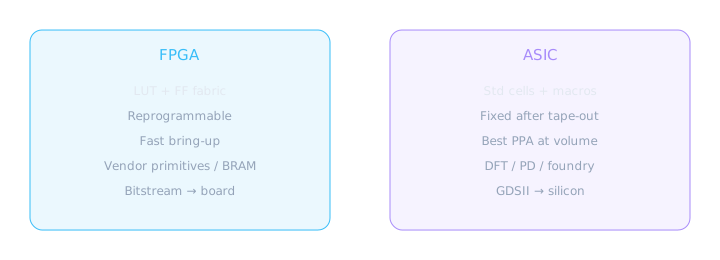
Same RTL skills; different finish line artifacts.
| Topic | FPGA | ASIC |
|---|---|---|
| Clocking | MMCM/PLL primitives, BUFG | PLL + clock tree synthesis |
| Memory | Infer BRAM / UltraRAM | Memory compiler macros |
| I/O | Bank standards, constraints file | Pad ring, ESD, IBIS |
| Timing sign-off | Vendor timing reports | STA corners + SI |
| Bug fix | New bitstream | Metal ECO or respin $$$ |
RTL that ports well
- Synchronous design with clear clock enables
- No delays (
#) in RTL — TB only - Avoid vendor primitives until the boundary wrapper
- Infer memories with portable templates when possible
- Document CDC and resets the same way for both
// Portable synthesizable counter — FPGA or ASIC friendly
module portable_counter #(
  parameter WIDTH = 8
)(
  input  wire             clk,
  input  wire             rst_n,
  input  wire             en,
  output reg  [WIDTH-1:0] count
);
  always @(posedge clk or negedge rst_n) begin
    if (!rst_n) count <= {WIDTH{1'b0}};
    else if (en) count <= count + {{(WIDTH-1){1'b0}}, 1'b1};
  end
endmodule
Copy-pasting Xilinx/Intel primitive instantiations into an ASIC flow (or the reverse) locks you in. Keep a thin fpga_clk_wrap / asic_clk_wrap at the top.
Soft CPU on FPGA vs custom silicon on ASIC
Same problem — “run firmware” — different platform trade-offs:
FPGA: soft processor
Drop in MicroBlaze, Nios II, or RISC-V soft core. Recompile bitstream to change RTL around it. Great for prototypes, low volume, fast iteration.
ASIC: hard / custom core
License ARM/RISC-V hard macro or design your own. Best MHz/mm²/W at millions of units. Months to tape-out; bugs are expensive.
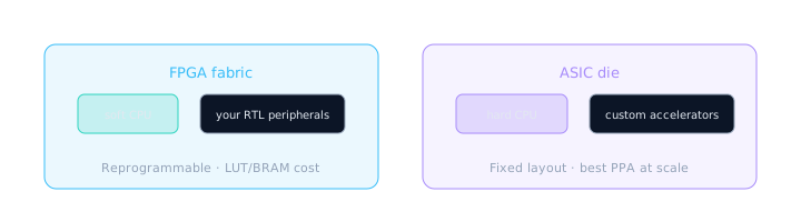
FPGA: CPU is RTL like everything else. ASIC: CPU is often a hardened block next to your logic.
<10k units, specs still changing → FPGA (maybe soft CPU). >100k units, cost/power critical → ASIC. Your RTL style stays the same; the wrapper and constraints change.
Constraint files — telling tools about clocks & pins
RTL alone does not know board clock frequency or pin locations. Constraint files bridge RTL to physical reality:
- FPGA (Xilinx):
.xdc— pin LOC,create_clock, I/O standards. - FPGA (Intel):
.sdc— same ideas, Quartus syntax. - ASIC:
.sdc(Synopsys Design Constraints) — clocks, input/output delays, false paths.
| Constraint | FPGA (XDC) | ASIC/FPGA (SDC) |
|---|---|---|
| Define clock | create_clock -period 10 [get_ports clk] | create_clock -name clk -period 10 [get_ports clk] |
| Pin location | set_property PACKAGE_PIN W5 [get_ports clk] | N/A (ASIC: floorplan) |
| I/O delay | set_input_delay / set_output_delay | Same — models board/setup |
| False path | set_false_path -from [get_ports rst_n] | set_false_path -from [get_ports por_n] |
# --- Xilinx Vivado (.xdc) snippets ---
create_clock -period 10.000 -name sys_clk [get_ports clk_50m]
set_property PACKAGE_PIN W5 [get_ports clk_50m]
set_property IOSTANDARD LVCMOS33 [get_ports clk_50m]
set_input_delay -clock sys_clk -max 2.0 [get_ports data_in[*]]
set_output_delay -clock sys_clk -max 2.0 [get_ports data_out[*]]

# --- Synopsys / Intel / ASIC STA (.sdc) snippets ---
create_clock -name clk -period 8.0 [get_ports clk]
set_input_delay  1.5 -clock clk [all_inputs]
set_output_delay 1.5 -clock clk [all_outputs]
set_false_path -from [get_ports rst_n]
set_multicycle_path 2 -setup -from [get_cells div/*] -to [get_cells quot_reg*]

# RTL does not contain these — they ship beside the design per target
Course note: Browser labs skip constraints (no pins, ideal clock). Real FPGA/ASIC flows fail timing reports without them.
Flow diagram
// Conceptual — keep platform specifics at the edge
module clk_wrap (
  input  wire clk_pad,
  output wire clk_sys
);
  // `ifdef FPGA
  //   BUFG u_buf (.I(clk_pad), .O(clk_sys));
  // `else
  //   // ASIC: clock buffer / CTS leaf handled by tools
       assign clk_sys = clk_pad;
  // `endif
endmodule
How this course uses both ideas
Labs run in the browser simulator (ASIC/FPGA agnostic). Coding style aims at synthesis-friendly RTL that would map to either. Module 9 adds timing/area thinking that ASIC teams live in — and FPGA timing reports still reward.
Job posts saying “FPGA” or “ASIC RTL” both expect: flops, FSMs, lint, CDC awareness, and waveform debug. Platform IP is learnable; bad digital fundamentals are not.
Module 2 checkpoint
- I can reason about bit widths and overflow
- I can tell combo from sequential in code and waves
- I understand setup/hold at intuition level
- I can write a clean reset flop template
- I can narrate a simple timing diagram
- I know FPGA vs ASIC differences without panic
- I know when soft CPU (FPGA) vs hard/custom (ASIC) fits
- I've seen XDC/SDC constraint one-liners
Up next — Module 3: Verilog from Scratch — modules, always blocks, blocking vs non-blocking as language law.
🎯 What to remember
- Same synthesizable RTL core; different wrappers and sign-off.
- Portability = sync style + no TB-only constructs in RTL.
- Constraints (.xdc / .sdc) tell tools clock period and pin timing.
- Module 2 complete — digital foundations unlocked.
- Continue from the course index into Module 3 when published.