Why multi-clock chips exist (CDC mindset for designers)
No real SoC runs on one clock. CPUs, DRAM, PCIe, and sensor blocks each need their own frequency — and every boundary between them is a CDC problem you must design, not hope DV finds.
A signal generated in clock domain A sampled by logic in clock domain B without a guaranteed phase relationship. Without proper synchronizers, metastability can corrupt data.
Why SoCs are multi-clock
A single global clock at max frequency would burn power and fail timing on slow peripherals. Engineers partition by function and pick the slowest clock that meets each block's throughput target.
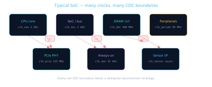
Power, timing, and protocol requirements force multiple clocks. Integration creates dozens of CDC interfaces.
Power
Slower clocks = lower dynamic power. Gate domains independently.
Protocol
PCIe, DDR, UART each mandate specific frequencies.
Timing
Not every path needs 2 GHz. Partition by criticality.
| Block | Typical clock | Why separate |
|---|---|---|
| CPU core | High (GHz) | Performance-critical compute |
| Peripheral bus | Medium (100s MHz) | GPIO, SPI, I2C don't need GHz |
| Always-on | Low (kHz) | Wake logic runs while main core sleeps |
| PHY interfaces | Protocol-defined | Cannot be arbitrarily changed |
Metastability — the physical problem
When a signal changes near the receiving clock edge, the capturing flop may enter a metastable state — output neither solid 0 nor 1 for an unbounded (but exponentially unlikely) time. One bad sample can corrupt a state machine or counter.
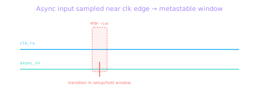
Simulation models metastability as zero-delay or X-prop — neither matches silicon. A CDC bug can pass 100% sim coverage and still fail in the field.
# Block CDC interface table (required in every block spec)
| Signal      | Dir | Width | Src clk   | Dst clk   | Structure      | Latency |
|-------------|-----|-------|-----------|-----------|----------------|---------|
| irq_periph  | in  | 1     | clk_periph| clk_cpu   | 2-flop sync    | 2+ cyc  |
| cfg_update  | in  | 32    | clk_cpu   | clk_periph| toggle handshake| 4+ cyc |
| dma_ptr     | out | 8     | clk_cpu   | clk_ddr   | Gray + 2FF     | 2+ cyc  |
CDC is a design concern — not only DV
Verification can inject random metastability and run formal CDC tools — but someone must write the synchronizer RTL first. That someone is the designer at the domain boundary.
| Role | CDC responsibility |
|---|---|
| RTL designer | Choose sync structure (2FF, pulse, handshake, FIFO) |
| Integration lead | Map all crossings; ensure SDC clock groups match |
| DV engineer | CDC-focused sim, protocol checkers, coverage of crossings |
| Signoff | SpyGlass CDC / Jasper formal CDC — lint + structural proof |
// BAD — designer throws signal across domains, hopes DV catches it
// In clk_cpu domain:
reg irq_cpu;
always @(posedge clk_cpu) irq_cpu <= peripheral_irq;  // async!

// BAD — multi-bit bus without gray/FIFO
always @(posedge clk_sys)
  status_vec <= counter_from_slow_clk;  // bits arrive at different times
// GOOD — designer owns the crossing
// 1-bit level: 2-flop sync (lesson 9.6)
reg irq_meta, irq_sync;
always @(posedge clk_cpu or negedge rst_n) begin
  if (!rst_n) {irq_meta, irq_sync} <= 2'b00;
  else        {irq_meta, irq_sync} <= {peripheral_irq, irq_meta};
end

// Multi-bit counter: gray-code sync or async FIFO
// See /premium-course/cdc/ for full patterns
The EcrioniX CDC course covers MTBF math, gray-code pointers, async FIFOs, and formal signoff. This module gives you the designer mindset; that course gives you depth.
Designer CDC checklist at block boundaries
- Document every output that leaves your clock domain
- 1-bit levels → 2-flop synchronizer in receiving domain
- Pulses → pulse synchronizer (not raw 2FF on a 1-cycle pulse)
- Multi-bit data → handshake, gray counter, or async FIFO
- Never synchronize a bus bit-by-bit with separate 2FF chains
- Add
CDC_SYNCcomments lint tools can match - Run CDC lint before handing block to integration
Frequency ratios and clock relationships
Not all multi-clock systems are fully asynchronous. Understanding the relationship between domains helps pick synchronizers and set constraints.
| Relationship | Example | Design note |
|---|---|---|
| Synchronous | clk and clk/2 from same PLL | STA handles; still document phase |
| Rational | 100 MHz and 25 MHz (÷4) | May use simpler sync; verify with STA |
| Asynchronous | CPU clk + crystal UART | Full 2FF / handshake / FIFO required |
| Gated / dynamic | Power-gated domain | Isolation + retention; RDC lint |
Assuming two clocks are "close enough" because they're both on the chip. If they come from different oscillators or PLL outputs with no phase lock, treat them as asynchronous.
Reset-domain crossing (RDC): Async reset deassert without synchronizer is a cousin of CDC. Lint tools (Questa RDC, SpyGlass) flag reset paths that cross domains unsynchronized — same designer-owned mindset applies.
From mindset to structures
Lesson 9.6 gives you the decision table: when to use 2-flop sync, pulse sync, or req/ack handshake — with code and diagrams. The rule of thumb: match the synchronizer to the signal type, not the other way around.
Document crossings
Every CDC interface gets a row in your block spec: signal, width, structure, latency.
Lint early
Run CDC lint on your block before integration — don't wait for SoC signoff.
Go deeper
MTBF math, gray pointers, formal CDC → CDC course.
// Integration view — designer owns synchronizer inside boundary
module uart_top (
  input  wire       clk_cpu,
  input  wire       clk_uart,   // async to cpu
  input  wire       rst_n,
  input  wire       tx_valid_cpu,
  input  wire [7:0] tx_data_cpu,
  output wire       tx_busy_cpu
);
  // All clk_uart ↔ clk_cpu crossings use named sync modules
  sync_2ff      u_busy_sync  (.clk_dst(clk_cpu), ...);
  pulse_sync    u_tx_pulse   (.clk_src(clk_cpu), .clk_dst(clk_uart), ...);
  // Never: assign tx_data_uart = tx_data_cpu;  // raw bus — lint ERROR
endmodule
These five checkboxes are what integration leads verify when your block connects to the SoC. Fill them in proactively — don't wait for CDC lint to find gaps.
🎯 What to remember
- Multi-clock SoCs are mandatory — power, protocol, and timing demand it.
- Metastability is real; sim hides it. Design synchronizers, don't rely on luck.
- CDC is designer-owned at the boundary; DV and signoff verify your choices.
- 1-bit ≠ multi-bit — different sync structures for each.
- Next: 2-flop, pulse sync, and handshake — when to use which.