Register files & simple memories
Counters and shift registers store one value. A register file stores many — indexed by address with simultaneous read and write ports. Larger storage uses inferred SRAM from a Verilog array. This lesson covers the RTL patterns for both, and why ROM behaves differently from writable RAM.
Memory RTL = array of registers + address decode. Writes happen on clock edges with we; reads are either combinational (small regfile) or registered (sync RAM). ROM is a read-only array initialized at elaboration.
Register file — 1 write, 2 read ports
The classic CPU regfile: one write port (wb), two independent read ports (ra, rb). Reads are typically combinational from the stored array; write occurs on the clock edge.
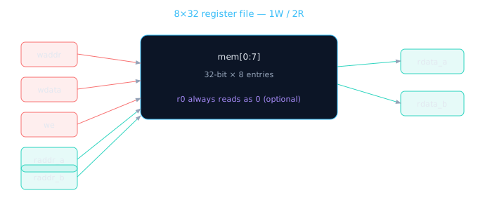
Write is clocked; reads are combinational mux from the array (async read port).
module regfile_1w2r #(
  parameter ADDR_W = 3,   // 8 entries
  parameter DATA_W = 32
) (
  input  wire                  clk,
  input  wire                  rst_n,
  input  wire                  we,
  input  wire [ADDR_W-1:0]     waddr,
  input  wire [DATA_W-1:0]     wdata,
  input  wire [ADDR_W-1:0]     raddr_a,
  input  wire [ADDR_W-1:0]     raddr_b,
  output wire [DATA_W-1:0]     rdata_a,
  output wire [DATA_W-1:0]     rdata_b
);
  localparam DEPTH = 1 << ADDR_W;
  reg [DATA_W-1:0] mem [0:DEPTH-1];

  // Async read (combinational)
  assign rdata_a = (raddr_a == {ADDR_W{1'b0}}) ? {DATA_W{1'b0}} : mem[raddr_a];
  assign rdata_b = (raddr_b == {ADDR_W{1'b0}}) ? {DATA_W{1'b0}} : mem[raddr_b];

  integer i;
  always @(posedge clk or negedge rst_n) begin
    if (!rst_n) begin
      for (i = 0; i < DEPTH; i = i + 1)
        mem[i] <= {DATA_W{1'b0}};
    end else if (we && (waddr != {ADDR_W{1'b0}}))
      mem[waddr] <= wdata;
  end
endmodule
A register file is a bank vault with numbered boxes. Two people can look into different boxes simultaneously (read ports), but only one person can deposit per clock tick (write port).
Synchronous RAM — inference sketch
For larger memories, register both address and data. Synthesis infers block RAM (BRAM on FPGA, SRAM macro on ASIC).
module sync_ram #(
  parameter ADDR_W = 10,  // 1024 deep
  parameter DATA_W = 32
) (
  input  wire                  clk,
  input  wire                  we,
  input  wire [ADDR_W-1:0]     addr,
  input  wire [DATA_W-1:0]     wdata,
  output reg  [DATA_W-1:0]     rdata
);
  localparam DEPTH = 1 << ADDR_W;
  reg [DATA_W-1:0] mem [0:DEPTH-1];

  always @(posedge clk) begin
    if (we)
      mem[addr] <= wdata;
    rdata <= mem[addr];   // read data registered — 1-cycle latency
  end
endmodule
Read-during-write behavior is undefined unless you specify write-first or read-first policy. Document which value rdata returns when we and read share the same address.
ROM vs RAM — async read
| Property | RAM (sync) | ROM (async read) |
|---|---|---|
| Writable | Yes (we) | No — initialized at compile |
| Read timing | Registered (1+ cycle) | Combinational from array |
| Inference | BRAM / SRAM macro | LUT-ROM / mask ROM |
| Typical size | KB–MB | Small lookup tables, microcode |
module async_rom #(
  parameter ADDR_W = 4,
  parameter DATA_W = 16
) (
  input  wire [ADDR_W-1:0]     addr,
  output wire [DATA_W-1:0]     rdata
);
  reg [DATA_W-1:0] mem [0:(1<<ADDR_W)-1];

  initial begin
    mem[0]  = 16'h0000;
    mem[1]  = 16'h0001;
  // ... fill via $readmemh("rom.hex", mem) in real designs
  end

  assign rdata = mem[addr];  // combinational read — OK for ROM
endmodule
Rule of thumb: Small regfile (<32 entries) → flip-flop array with async read. Large memory (>256 entries) → sync RAM with registered read. Lookup tables / sin/cos → ROM.
Memory design checklist
- Document read latency (0-cycle async vs 1-cycle sync)
- Define read-during-write policy for shared addresses
- Hardwire r0=0 if your ISA requires it — block writes to address 0
- Use
$readmemhfor ROM init — don't hand-code large tables - Reset all RAM entries if your verification environment requires known state
🎯 What to remember
- Regfile = small multi-ported array; async read + clocked write is the CPU pattern.
- Sync RAM = registered read/write; synthesis infers block memory.
- ROM = fixed content, combinational read is fine — never use async read for writable RAM at scale.
- Address 0 conventions and write-enable gating matter as much as the array itself.