Shift registers & serial/parallel conversion
A shift register is a chain of flip-flops where each stage passes its value to the next on every clock edge. By choosing what goes in (serial or parallel) and what you read out, you get four classic modes — SIPO, PISO, SISO, and PIPO — that underpin SPI, UART, scan chains, and delay lines.
Shift register RTL is a concatenation shift: shift_reg <= {shift_reg[WIDTH-2:0], serial_in}. Load parallel data when load is asserted; otherwise shift.
Four shift-register modes
| Mode | Data in | Data out | Typical use |
|---|---|---|---|
| SIPO | 1 bit serial | N bits parallel | SPI slave receive, deserialize |
| PISO | N bits parallel | 1 bit serial | SPI master transmit, serialize |
| SISO | 1 bit | 1 bit (other end) | Delay line, scan chain |
| PIPO | N bits | N bits (shifted) | Barrel shift, pipeline delay |
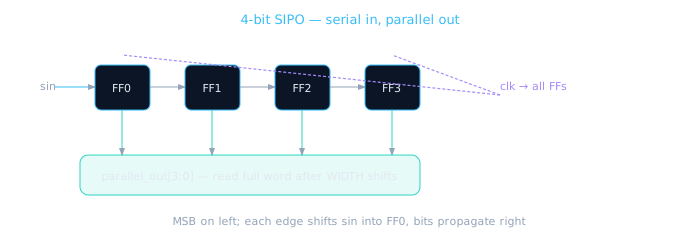
SIPO: shift in one bit per clock; after N cycles the full word is available in parallel.
A shift register is a conveyor belt of boxes. SIPO drops one marble in at a time and reads all boxes at once. PISO loads all boxes at once and removes marbles one at a time from the end.
SIPO & PISO RTL
module sipo #(
  parameter WIDTH = 8
) (
  input  wire             clk,
  input  wire             rst_n,
  input  wire             shift_en,
  input  wire             serial_in,
  output reg  [WIDTH-1:0] parallel_out
);
  always @(posedge clk or negedge rst_n) begin
    if (!rst_n)
      parallel_out <= {WIDTH{1'b0}};
    else if (shift_en)
      parallel_out <= {parallel_out[WIDTH-2:0], serial_in};
  end
endmodule
module piso #(
  parameter WIDTH = 8
) (
  input  wire             clk,
  input  wire             rst_n,
  input  wire             load,       // parallel load
  input  wire             shift_en,
  input  wire [WIDTH-1:0] parallel_in,
  output wire             serial_out
);
  reg [WIDTH-1:0] shift_reg;

  always @(posedge clk or negedge rst_n) begin
    if (!rst_n)
      shift_reg <= {WIDTH{1'b0}};
    else if (load)
      shift_reg <= parallel_in;
    else if (shift_en)
      shift_reg <= {shift_reg[WIDTH-2:0], 1'b0};
  end

  assign serial_out = shift_reg[WIDTH-1];  // MSB out first
endmodule
Define bit order (MSB-first vs LSB-first) in your spec. SPI and UART disagree — document which end serial_out taps.
Universal shift register (load + shift)
Real designs combine parallel load and serial shift in one register — the pattern behind scan chains and configurable IO.
module universal_shift #(
  parameter WIDTH = 8
) (
  input  wire             clk,
  input  wire             rst_n,
  input  wire             load,
  input  wire             shift_en,
  input  wire             serial_in,
  input  wire [WIDTH-1:0] parallel_in,
  output reg  [WIDTH-1:0] parallel_out,
  output wire             serial_out
);
  always @(posedge clk or negedge rst_n) begin
    if (!rst_n)
      parallel_out <= {WIDTH{1'b0}};
    else if (load)
      parallel_out <= parallel_in;
    else if (shift_en)
      parallel_out <= {parallel_out[WIDTH-2:0], serial_in};
  end
  assign serial_out = parallel_out[WIDTH-1];
endmodule
LFSR — light introduction
A Linear Feedback Shift Register XORs selected tap bits and feeds the result back into the serial input. With the right polynomial it cycles through 2N−1 states — a compact pseudo-random source for BIST and scrambling.
module lfsr4 (
  input  wire       clk,
  input  wire       rst_n,
  input  wire       en,
  output reg  [3:0] lfsr_out
);
  wire feedback = lfsr_out[3] ^ lfsr_out[2];  // polynomial x^4+x^3+1

  always @(posedge clk or negedge rst_n) begin
    if (!rst_n)
      lfsr_out <= 4'b0001;   // non-zero seed required
    else if (en)
      lfsr_out <= {lfsr_out[2:0], feedback};
  end
endmodule
Scan chains (Module 1.6 DFT) are shift registers wired through every flip-flop. LFSRs generate test patterns fed into those chains. Same primitive, different application.
Shift register checklist
- Document MSB-first vs LSB-first shift direction
- Separate
loadandshift_en— never shift and load on same edge without spec clarity - Non-zero LFSR seed — all-zero state is a stuck point for standard XOR LFSRs
- Count cycles: SIPO needs WIDTH shifts before parallel word is valid
- PIPO is just a register with concatenation shift — no serial port needed
🎯 What to remember
- Shift register = chained FFs +
{reg[MSB-1:0], sin}concatenation. - SIPO deserializes; PISO serializes — the bridge between slow serial buses and wide parallel datapaths.
- Universal shift = load OR shift — one module, two modes.
- LFSR = shift register + XOR feedback — pseudo-random patterns for test and link scrambling.