What is a chip, really? Idea → packaged silicon
A chip is not “magic sand.” It is a carefully planned product that moves from an idea, through design and manufacturing, into a package that sits on a board. This lesson gives you the story of that journey so every later module has a home.
VLSI (Very Large Scale Integration) means putting millions/billions of transistors on one die — and organizing teams + tools so that complexity stays manageable.
The VLSI journey — this course lives mainly in the highlighted RTL stage, with awareness of everything around it.
From idea to thing you can hold
- Need — a product goal (“talk to sensors over I2C”, “decode video”, “run Linux”).
- Specification — written requirements: features, speed, power, interfaces, cost.
- Architecture — big blocks and how they talk (still mostly diagrams).
- RTL design — Verilog/SystemVerilog that describes the digital behavior.
- Verification — prove the RTL matches the intent (tests, bugs, coverage).
- DFT — hooks so factories can test manufactured chips.
- Synthesis — RTL becomes a gate-level netlist for a chosen technology.
- Physical design — place gates, route wires, meet timing on a real die.
- Sign-off & tape-out — final checks; then manufacturing.
- Package & board — die in a package, soldered onto a PCB, shipping to customers.
Spec is the building code + customer brief. Architecture is the floor plan. RTL is the detailed construction drawings for the digital “rooms.” PD is pouring concrete and running plumbing. Tape-out is when the city permits construction.
RTL is just text that describes hardware. Here is a tiny taste — a 1-bit register. You will write many like this later.
// A 1-bit register — the simplest "chip building block"
module tiny_reg (
  input  wire clk,
  input  wire rst_n,
  input  wire d,
  output reg  q
);
  always @(posedge clk or negedge rst_n) begin
    if (!rst_n)
      q <= 1'b0;
    else
      q <= d;
  end
endmodule
Another taste — a simple 2:1 mux. Hardware is parallel: both inputs exist at once; sel picks which path feeds the output.
module mux2_taste (
  input  wire a,
  input  wire b,
  input  wire sel,
  output wire y
);
  assign y = sel ? b : a;  // combo logic — no clock needed
endmodule
Each stage: artifacts, owners, and what breaks if you skip it
Every box in the flow rail produces deliverables someone signs off on. Skipping a stage does not remove the work — it moves the pain later.
| Stage | Typical artifacts | Who owns it | If skipped / rushed |
|---|---|---|---|
| Spec | Requirements doc, interface tables, acceptance tests | Systems / product / architect | RTL rewrites, scope fights, “works on my bench” |
| Architecture | Block diagram, clock map, register outline | Architect + leads | Spaghetti interfaces, surprise CDC, PD nightmares |
| RTL | Verilog/SV, lint-clean, unit TB | RTL designer (you) | Nothing to verify or synthesize |
| Verify | Test plan, coverage, bug database | DV engineer + designer | Silent silicon bugs, recall risk |
| DFT | Scan chains, ATPG patterns, BIST hooks | DFT engineer | Low yield, expensive manual test, scrap die |
| Synthesis | Gate netlist, area/timing reports | RTL + synthesis engineer | No physical starting point, wrong timing assumptions |
| PD | Placed/routed layout, CTS, congestion reports | Physical designer | Timing fails, unroutable design, hot spots |
| Sign-off | STA, DRC, LVS, power sign-off decks | PD + STA + sign-off lead | Foundry reject, dead chips, schedule slip |
| Package / board | BGA footprint, PCB layout, bring-up plan | Package + HW engineer | Chip works in lab sim but not on customer board |
When someone says “can we skip verification and fix in silicon?” — translate that to schedule + money + reputation risk. A respin can cost millions and months; a week of directed tests rarely does.
Where time and money actually go
Beginners picture “writing Verilog” as most of the job. In practice on a modern SoC:
- Verification often consumes 50–70% of engineering hours before tape-out.
- NRE (non-recurring engineering) for ASIC — mask sets, EDA licenses, foundry setup — can be $1M–$50M+ before unit one ships.
- RTL + integration is intense but usually not the majority of calendar time on large chips.
- PD + sign-off iterations can dominate the last months of a program (“timing closure hell”).
Why this matters to you: writing clean, verifiable RTL early saves verification and PD time downstream — that is how junior engineers become trusted quickly.
VLSI vocabulary (Module 1 cheat sheet)
| Term | One-line meaning |
|---|---|
| Die | The silicon chip before packaging |
| Netlist | Gate-level connectivity after synthesis |
| Tape-out | Release design to foundry for masks |
| NRE | One-time cost before first unit ships |
| Yield | % of manufactured die that pass test |
| ECO | Engineering change order — late fix |
Worked mini-example — tracing one bug backward
Symptom: I2C sensor read returns 0xFF on silicon but passes in sim.
- Verify: Was NACK path tested? (often no → spec gap)
- RTL: Open-drain SDA drive strength wrong?
- PD: Pad cell wrong voltage domain?
- Board: Missing external pull-up resistor?
Notice how the flow helps you ask structured questions instead of random guessing.
ASIC vs FPGA (same ideas, different finish)
ASIC
Custom silicon. Long NRE cost, best power/perf/cost at volume. Flow includes foundry tape-out.
FPGA
Reconfigurable fabric. Faster bring-up, great for learning and prototypes. Still needs good RTL + timing thinking.
| Dimension | ASIC | FPGA |
|---|---|---|
| Unit cost at volume | Lowest (cents–dollars) | Higher (part cost + power) |
| Up-front cost | High NRE (masks, tools) | Low (dev board + license) |
| Time to first working chip | Months–years | Days–weeks |
| Clock speed / power | Optimized for product | Good, rarely best-in-class |
| Change after “ship” | ECO or respin ($$$) | Re-bitstream (minutes) |
| DFT / manufacturing test | Scan, ATPG, ATE mandatory | Functional test on board |
| Sign-off artifacts | STA, DRC, LVS, IR drop | Timing report + bitstream |
| RTL you write | Same synthesizable style — clarity, reset, clocks | |
“When would you choose FPGA vs ASIC?” — Good answer mentions volume, power budget, time-to-market, and change frequency. Prototype on FPGA; productize in ASIC when economics justify NRE.
This course teaches RTL that is honest for both worlds. Tool screenshots may differ; the engineering thinking does not.
From die to something on your desk
A “chip” is not one object — it is a stack of physical layers:
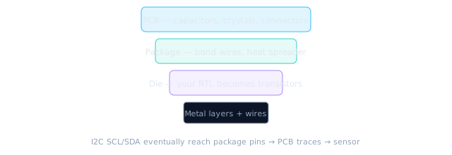
RTL describes behavior on the die; PD and IO cells connect it to the outside world.
Simulating RTL without thinking about pads, package, and board is fine for learning — but production bugs often live at the boundary (wrong IO standard, missing pull-up, reset sequencing).
Where YOU will live
Most of this course sits in RTL design + verification habits, with enough Spec/Arch/DFT/PD awareness that you never feel lost in meetings.
- You will write and simulate RTL in the online Verilog simulator
- You will learn what happens after RTL (so your code is synthesis- and PD-friendly)
- You will finish with an I2C design you can explain Spec → waves
- You will speak the vocabulary of meetings: STA slack, scan, floorplan, acceptance test
Mini worked example — reading the flow for one sentence of product need:
Need: “Read a temperature sensor over I2C.” That one line becomes: I2C master spec → CSR map architecture → RTL FSM → directed TB → scan-friendly flops → synthesis constraints → IO placement near sensor pins → STA on pad paths.
🎯 What to remember
- A chip is a long pipeline of roles — Spec, Arch, RTL, Verify, DFT, Synthesis, PD, Sign-off.
- RTL is the digital blueprint; silicon is the built house.
- ASIC and FPGA share RTL skills; manufacturing differs.
- Next: how to write a specification that design can actually implement.