Clock & reset lint rules that matter
Clock and reset topology determines whether STA closes and whether silicon powers up reliably. Lint enforces rules that simulation often hides: clock used as data, gated clocks in RTL, async reset release, and mixed clock edges in one module.
All flops clocked by the same clock source (after defined tree/buffering). Crossing between domains without synchronizers is a CDC violation — lint flags it before STA does.
Clock used as data — CLK_AS_DATA
Using a clock signal as a logic input (enable, mux select, data) creates paths that STA treats differently from functional logic. The flop may see glitches; hold time becomes unpredictable.
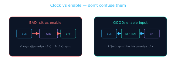
// BAD — clock bit used as data/enable
always @(posedge clk)
  if (clk) status <= irq;        // clk is always 1 at posedge → lint error

wire gated_clk = clk & enable;   // manual clock gate in RTL
always @(posedge gated_clk)       // lint: GATED_CLOCK
  count <= count + 1;
// GOOD — clock only on clock pin; enable on data path
always @(posedge clk) begin
  if (!rst_n)      count <= 8'h00;
  else if (enable) count <= count + 1;  // enable is data, not clock
end

// Clock gating: let synthesis/ICC insert ICG cells
// RTL uses enable-style; don't AND clk in Verilog
Gated clocks in RTL
Manually gating clk with an AND/OR in RTL bypasses the clock tree methodology. Modern flows use integrated clock gating (ICG) cells inserted by synthesis or PD. Lint flags assign gclk = clk & en patterns.
| Pattern | Lint severity | Correct approach |
|---|---|---|
assign gclk = clk & en | ERROR | Clock-enable flop or synthesis ICG |
always @(posedge (clk&en)) | ERROR | if(en) inside posedge clk |
| Latch-based ICG in RTL | WARNING | Use vendor ICG cell or enable FF |
Gated clocks "work" in simulation because the simulator happily toggles your AND gate. Silicon needs glitch-free clock enables and proper hold on the enable pin — that's why lint blocks RTL clock gates.
Async reset release
Asynchronous reset assertion is fine — reset immediately. De-assertion must be synchronous to the clock domain or you risk recovery/removal metastability. Lint flags reset removed mid-cycle.
Async assert (OK): flops reset immediately
Async deassert (BAD): release near clk edge → metastability
Sync deassert (GOOD): rst_n_async → [2FF sync] → rst_n_sync → used in always block
// Async assert, sync deassert — lint-approved pattern
module reset_sync (
  input  wire clk,
  input  wire rst_n_async,  // from pad / POR
  output wire rst_n_sync
);
  reg [1:0] sync_ff;
  assign rst_n_sync = sync_ff[1];

  always @(posedge clk or negedge rst_n_async) begin
    if (!rst_n_async)
      sync_ff <= 2'b00;           // async assert — immediate
    else
      sync_ff <= {sync_ff[0], 1'b1}; // sync release — 2 cycles
  end
endmodule

// Downstream logic uses rst_n_sync only
always @(posedge clk) begin
  if (!rst_n_sync) state <= IDLE;
  else             state <= next_state;
end
Review Reset Synchronizers and Sync vs Async Reset for the full reset methodology. Lint enforces what those lessons teach.
Mixed clock edges
Using both posedge clk and negedge clk in the same module creates half-cycle paths that are painful to constrain and verify. Lint flags MIXED_CLOCK_EDGE unless explicitly waived for DDR IO.
// BAD — posedge and negedge in same module for "free" half-cycle
always @(posedge clk) capture <= data_in;
always @(negedge clk) process  <= capture + 1;  // half-cycle path

// GOOD — single edge; pipeline if you need more time
always @(posedge clk) begin
  capture <= data_in;
  process <= capture + 1;  // 1-cycle latency, clean timing
end
| Rule | Why lint cares |
|---|---|
| One edge per domain per module | Simplifies SDC constraints |
| No derived clocks in RTL | STA needs SDC clock definitions |
| Reset async assert / sync deassert | Prevents reset-induced metastability |
| No clock on non-clock pins | Prevents glitch-sensitive logic |
SDC alignment — lint and STA must agree
Lint tools read your SDC (Synopsys Design Constraints) to identify clock domains. If RTL names a clock clk_uart but SDC calls it uart_clk, lint may flag false CDC crossings or miss real ones.
# SDC must match RTL port names exactly
create_clock -name clk_cpu   -period 0.5  [get_ports clk_cpu]
create_clock -name clk_uart  -period 8680 [get_ports clk_uart]
set_clock_groups -asynchronous \
  -group [get_clocks clk_cpu] \
  -group [get_clocks clk_uart]

# False path ONLY on synchronizer chains — not on data paths
set_false_path -from [get_cells sync_meta_reg] -to [get_cells sync_sync_reg]
Lint + SDC + RTL form a triangle. Change any leg without updating the others and signoff breaks. Keep a clocks.md in your block doc listing every domain and its SDC name.
// DFT: scan mode bypasses ICG — designer must not block this
// Synthesis inserts: ICG with test_en pin
// RTL author: use enable style; never manual clk gate
// Lint: verify scan_en reaches ICG (DFT team validates)

// Your job: don't gate flops that must be scannable without DFT review
// e.g. TAP controller, boundary scan — always-on during test
Clock/reset lint checklist
- Every sequential block uses exactly one clock edge per domain
- Clock signals connect only to clock pins — never as data or enable
- No manual
clk & engating in RTL — use enable flops - Async resets pass through synchronizer before deassert to logic
- SDC file defines every clock lint sees in RTL
- Cross-domain paths flagged — covered in lessons 9.5–9.6
- Review clock/reset lint after every RTL change — not only at milestone
| Lint rule | Typical message | Fix in one line |
|---|---|---|
CLK_AS_DATA | Clock used as data input | Use enable, not clk, as condition |
GATED_CLOCK | Combo clock gate inferred | if(en) inside posedge clk |
RST_SYNC_RELEASE | Async reset deassert unsync | reset_sync module per domain |
MIXED_CLOCK_EDGE | posedge + negedge same module | Pipeline to single edge |
// Clock muxing is a PD/signoff topic — NOT done in RTL at block level
// Lint flags: CLOCK_MUX_IN_RTL
// Correct: two separate clock inputs, select in clock controller IP
// Block RTL uses clk_selected as input port — does not generate it

module my_block (
  input wire clk,       // already-muxed clock from CRG
  input wire rst_n_sync // already-synchronized reset
);
  // Designer never muxes clocks here
endmodule
🎯 What to remember
- Clock is infrastructure, not data. Enable flops, not AND gates on clk.
- Async reset assert OK; deassert must be synchronized per domain.
- Mixed posedge/negedge in one block is a timing trap — pipeline instead.
- Lint clock rules align with STA assumptions — ignore them and synthesis lies.
- Next: how to read lint reports and fix root causes instead of waiving.