I2C master architecture
Protocol knowledge from 11.1 and the micro-spec from 11.2 now become structure. A production I2C master splits into a CSR bank for software, a byte-level FSM for transactions, a bit engine for SCL timing, and an open-drain pad wrapper for the bus. This lesson defines every block, every interface, and the clock-stretch handshake that trips up first-time implementers.
Byte FSM thinks in transactions. Bit engine thinks in quarter-phases. Pads think in wired-AND. Keep these layers separate — mixing them produces unmaintainable RTL and untestable bugs.
Hierarchy and responsibilities
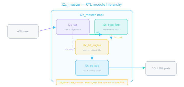
Commands flow down; status and sampled ACK flow up. Pad module is the only block that touches bidirectional pins.
| Module | Clock domain | Responsibility |
|---|---|---|
i2c_csr | pclk | Decode APB; latch ADDR, TX, DIV; expose STAT, RX; pulse START |
i2c_byte_fsm | pclk | Sequence START → addr → data → ACK → STOP; byte counter |
i2c_bit_engine | pclk | Generate SCL quarter-phases; shift one bit; sample ACK |
i2c_od_pad | async pins | Open-drain drive + synthesizable pull-up for sim |
Byte FSM — transaction states
The byte FSM is the orchestrator. It knows what to send (address, TX data, read phase) but delegates how to wiggle pins to the bit engine.
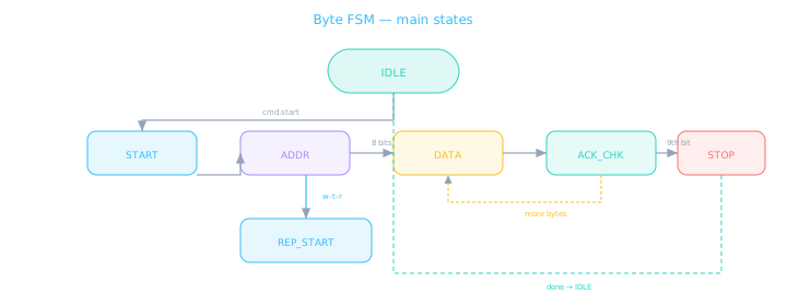
ACK_CHK branches: NACK → STOP (error); more bytes → DATA; last byte + read → master drives ACK/NACK.
| State | Entry action | Exit condition |
|---|---|---|
| IDLE | BUSY=0; release bus (oen=1) | CTRL.START pulse → START |
| START | bit_cmd=GEN_START | bit_done → ADDR (load shifted addr byte) |
| ADDR | Shift (addr<<1)|rd; 8 bits out | 8 bits done → ACK_CHK |
| DATA | Load TX or receive into shift reg | 8 bits done → ACK_CHK |
| ACK_CHK | Sample ack_bit on 9th rising edge | NACK → STOP; else byte_cnt-- → DATA or STOP |
| REP_START | bit_cmd=GEN_REP_START; flip rd bit | bit_done → ADDR or DATA |
| STOP | bit_cmd=GEN_STOP | bit_done → IDLE; DONE=1 |
// Byte FSM → Bit engine (command)
output reg        bit_go;
output reg [2:0]  bit_cmd;  // IDLE, START, STOP, REP_START, TX_BIT, RX_BIT
output reg        bit_wr;   // 1=master drives SDA this bit
output reg        tx_bit;   // data bit to transmit

// Bit engine → Byte FSM (status)
input  wire       bit_done;      // one bit (or START/STOP seq) complete
input  wire       ack_sample;    // SDA at 9th rising edge
input  wire       stretch_active; // SCL held low externally
Bit engine — quarter-phase timing
Each SCL period divides into four phases counted by a divider loaded from CSR DIV. This gives precise control over setup, sample point, and clock-stretch wait.
Quarter-phases within one bit (write data bit)

PH_HIGH is where clock stretch happens — phase counter pauses until scl_i == 1.
// Target f_scl = 400 kHz, pclk = 50 MHz
// DIV = 50_000_000 / (4 * 400_000) = 31.25 → use 31
// Actual f = 50M / (4*31) ≈ 403 kHz

localparam DIV_400K = 16'd31;

// In PH_HIGH: wait for external SCL release (clock stretch)
if (phase == PH_HIGH && !scl_i)
  phase_cnt <= phase_cnt;     // hold — do not advance
else if (phase_cnt == div_r - 1)
  phase_cnt <= 0; phase <= phase_next;
else
  phase_cnt <= phase_cnt + 1;
Open-drain pad model
The pad wrapper is the boundary between synchronous RTL and the asynchronous bus. In synthesis, it maps to tristate IO cells; in simulation, it models pull-ups.

oen_n active-low is common in pad libraries: 0 = drive low, 1 = high-Z.
Using assign sda_i = sda_pad without resolving Z to 1 hides the fact that nobody is driving. Always model pull-ups in TB and pad wrapper for accurate ACK/NACK and stretch behavior.
Clock stretching — wait for SCL high
When a slave is not ready, it holds SCL low after the master releases it. The master must not advance to the next bit or sample SDA until scl_i returns high. Stretching can occur during any SCL high phase — most commonly during ACK or while the slave prepares read data.
Clock stretch during ACK bit
- Detection: in PH_RISE or PH_HIGH, if master released SCL (oen=1) but
scl_i==0, stretch is active. - Response: freeze phase counter; do not increment bit index; assert
stretch_activefor debug. - Timeout (SHOULD): if stretch exceeds 25 ms at 400 kHz, abort and set STAT.ERR — prevents permanent hang.
Verification tip: directed test A5 from the 11.2 spec deliberately holds SCL low in TB. If your master completes without waiting, the bit engine PH_HIGH logic is broken.
CSR bank and interrupt logic
The CSR block bridges CPU clock domain and the FSM. Register offsets match Lesson 11.2; implementation lands in 11.4.
| Signal | Source | Consumer |
|---|---|---|
start_pulse | CTRL.START write-1 | Byte FSM: IDLE → START |
addr_r[6:0] | ADDR CSR | Byte FSM: forms addr byte |
div_r[15:0] | DIV CSR | Bit engine: phase length |
tx_data | TX CSR | Byte FSM: write payload |
rx_data | Byte FSM shift reg | RX CSR readback |
busy, done, nack | Byte FSM | STAT CSR; W1C on done/nack |
assign irq = irq_en & (stat_done | stat_nack | stat_timeout);

// Firmware ISR:
// 1. Read STAT
// 2. If NACK → handle error path
// 3. Write STAT to W1C clear done/nack
// 4. Read RX if read transaction
Interface contracts between blocks
Clear contracts let you unit-test each module in isolation before top-level integration.
| Boundary | Producer guarantees | Consumer assumes |
|---|---|---|
| CSR → FSM | START is a 1-cycle pulse; ADDR stable until BUSY | FSM ignores START when BUSY=1 |
| FSM → bit engine | bit_go pulse per bit; bit_cmd stable during bit | Engine completes with exactly one bit_done |
| bit engine → pads | SDA only changes in PH_SETUP or START/STOP seq | Pad resolves Z; returns scl_i/sda_i |
| bit engine → FSM | ack_sample valid only at end of 9th bit PH_HIGH | FSM latches ACK/NACK on bit_done |
Unit test bit engine
Feed bit_cmd sequences; check SCL/SDA waveforms without CSR or FSM present.
Unit test FSM
Stub bit_done/ack_sample; verify state transitions for A1–A4 scenarios.
Pad model TB
Two masters driving — verify wired-AND and stretch with conflicting oen.
Read path — shift register and master ACK
Write and read share the bit engine but differ in who drives SDA during data bits and who drives the 9th bit. The byte FSM must track rd_phase to swap drivers correctly.
| Phase | bit_wr | SDA driver (data bits) | 9th bit driver |
|---|---|---|---|
| ADDR (write) | 1 | Master | Slave ACK |
| ADDR (read) | 1 | Master | Slave ACK |
| DATA write | 1 | Master | Slave ACK |
| DATA read | 0 | Slave | Master ACK/NACK |
// In bit engine PH_HIGH during RX_BIT:
if (bit_cmd == RX_BIT)
  shift_reg <= {shift_reg[6:0], sda_i};  // MSB first

// Byte FSM during read ACK_CHK on last byte:
if (byte_cnt == 0)
  bit_wr <= 1; tx_bit <= 1;  // master NACK (release SDA → high)
else
  bit_wr <= 1; tx_bit <= 0;  // master ACK (pull SDA low)
START / STOP — bit engine sequences
START and STOP are not ordinary data bits — they violate the "change SDA only when SCL low" rule on purpose. The bit engine needs dedicated micro-sequences for these bus events.
| Event | SCL sequence | SDA sequence | Phase count |
|---|---|---|---|
| START | Hold high → fall → stay low | High → fall (while SCL high) → hold low | 3–4 custom phases |
| STOP | Rise → hold high | Low → rise (while SCL high) | 3–4 custom phases |
| REP_START | Same as START | Same as START (no prior STOP) | Reuse START seq |
| Data bit | Standard 4-phase | Setup in PH_SETUP | 4 × DIV |
START micro-sequence (conceptual)
typedef enum logic [2:0] {
  BIT_IDLE,
  BIT_START_SDA_FALL,  // SDA↓, SCL still high
  BIT_START_SCL_FALL,  // SCL↓
  BIT_PH_SETUP,
  BIT_PH_RISE,
  BIT_PH_HIGH,
  BIT_PH_FALL,
  BIT_STOP_SCL_RISE,   // SCL↑ first
  BIT_STOP_SDA_RISE    // SDA↑ while SCL high → bit_done
} bit_state_e;

// START entry: from BIT_IDLE when bit_cmd == GEN_START
// STOP entry: after last bit when bit_cmd == GEN_STOP
Reusing the data-bit FSM for START/STOP produces illegal intermediate states — SCL may fall before SDA, or SDA may glitch high during a data byte. Give START/STOP their own states.
Reset and bus-safe defaults
On reset, the I2C master must not leave the bus in an illegal state. A slave left mid-transaction may hang until it sees STOP.
- MUST Deassert all oen_n (release SCL and SDA) within 1 cycle of reset
- MUST Clear BUSY; byte FSM returns to IDLE
- SHOULD Optionally generate STOP if reset occurs mid-transaction (advanced — document if implemented)
- MAY Hold irq low during reset regardless of sticky STAT
always_ff @(posedge pclk or negedge preset_n) begin
  if (!preset_n) begin
    scl_oen_n <= 1'b1;   // release SCL
    sda_oen_n <= 1'b1;   // release SDA
    byte_state <= IDLE;
    busy       <= 1'b0;
  end
end
CDC note — async I2C pads
scl_i and sda_i are asynchronous to pclk — they can change at any time relative to the CPU clock. For a master that samples on internally generated SCL edges, you typically sample in PH_HIGH after sufficient delay, which provides implicit synchrony to your own clock generation.
- Do NOT double-flop
sda_ifor every bit without timing analysis — it adds metastability risk at the exact sample point. - DO sample only in PH_HIGH when your phase counter is near the end (stable bus after rise time).
- DO treat
scl_istretch detection as async: ifscl_i==0after release, wait — no edge sync needed. - If the I2C block runs from a separate clock (i2c_clk), synchronize
start_pulseand status back to pclk with pulse stretchers or APB handshake.
For this capstone, everything runs on pclk — the bit engine generates SCL as a logical output, and pad feedback is sampled mid-phase. Full CDC to a divided i2c_clk domain is an optional stretch goal, not required for sign-off.
Synthesis and constraints notes
The I2C master is a slow serial interface — timing closure is usually easy on pclk. The critical paths to watch are APB decode and the divider counter, not the pad outputs.
- False paths:
scl_i,sda_iare async inputs — do not time them to pclk without sync registers (and we intentionally sample mid-phase). - IO timing: pad cell insertion happens at top level; your RTL outputs
oen_nando— constrain in PAD .sdc separately. - Clock gating: MAY gate pclk to bit engine when IDLE to save dynamic power — ensure BUSY=0 and FSM in IDLE before gate enable drops.
- Lint: run clock-domain and reset checks; verify all FSM states have default recovery to IDLE on reset.
Synthesizing push-pull on SCL/SDA because the tool "optimizes away" tristate — force open-drain IO cell mapping in constraints or the chip will fight the bus.
Architecture review checklist
- Four modules: csr, byte_fsm, bit_engine, od_pad — clean hierarchy
- Byte FSM states cover START, ADDR, DATA, ACK_CHK, REP_START, STOP, IDLE
- Bit engine uses 4 quarter-phases; DIV register sets frequency
- PH_HIGH waits for scl_i during clock stretch; timeout optional
- Open-drain: oen_n=1 releases; Z resolves to 1 with pull-up model
- ACK sampled on 9th bit; NACK sets STAT and triggers STOP path
- Interface contracts documented between every block pair
- irq driven by done | nack | timeout with enable mask
- START/STOP have dedicated bit-engine states — not reused data-bit phases
- Read path: slave drives data; master drives 9th-bit ACK/NACK
- Reset releases bus (oen_n=1); FSM returns to IDLE
🎯 What to remember
- Layer separation: CSR (software), byte FSM (transactions), bit engine (timing), pads (electrical).
- Quarter-phase engine: setup → rise → high (sample + stretch wait) → fall.
- Clock stretch = freeze PH_HIGH until scl_i reads high — never skip this wait.
- Open-drain pads never drive high — only pull low or release to Z.
- Next lesson: RTL implementation (11.4) — turn this architecture into synthesizable Verilog.