I2C RTL implementation — byte engine + bit engine + CSR
Architecture from Lesson 11.3 is done — now you write the RTL. This lesson delivers paste-ready, synthesizable Verilog for the CSR map from Lesson 11.2, an open-drain bit engine, a byte-level FSM, and the top wrapper that ties them together. By the end you can simulate a single-byte write transaction.
Three layers: CSR (software interface), byte FSM (protocol sequencing), bit engine (SCL/SDA timing). Software writes ADDR + TXDATA, pulses START, polls STAT until DONE.
Three-layer block diagram
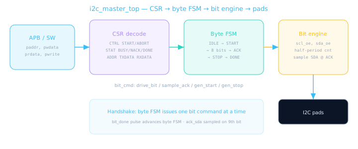
Software never touches SCL/SDA directly. CSR kicks the byte FSM; the bit engine owns pad timing.
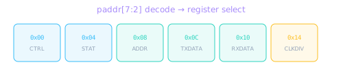
CSR map — matches Lesson 11.2
Byte-aligned 32-bit registers. CTRL bits are write-1-to-set or auto-clear on START; STAT is read-only status fed by the byte FSM.
| Offset | Name | Bits | Access | Description |
|---|---|---|---|---|
0x00 | CTRL | [0] START, [1] ABORT, [2] IRQ_EN | R/W | START auto-clears after accept; ABORT forces idle |
0x04 | STAT | [0] BUSY, [1] NACK, [2] DONE | R | BUSY high during transaction; DONE sticky until next START |
0x08 | ADDR | [6:0] 7-bit slave addr | R/W | Hardware shifts: write byte = {addr[6:0], 1'b0} — see 11.2 CSR map |
0x0C | TXDATA | [7:0] | R/W | Data byte to transmit after address |
0x10 | RXDATA | [7:0] | R | Captured read data (extension for read path) |
0x14 | CLKDIV | [15:0] | R/W | Half-period count in sys_clk cycles (default 50 → ~1 MHz @ 100 MHz) |
// i2c_csr.v — CSR map for I2C master (Lesson 11.2 compatible)
module i2c_csr #(
  parameter ADDR_W = 8
)(
  input  wire              clk,
  input  wire              rst_n,
  // Simple register bus (replace with APB in SoC)
  input  wire              reg_wr,
  input  wire              reg_rd,
  input  wire [ADDR_W-1:0] reg_addr,
  input  wire [31:0]       reg_wdata,
  output reg  [31:0]       reg_rdata,
  // To byte FSM
  output reg               ctrl_start,
  output reg               ctrl_abort,
  output reg               ctrl_irq_en,
  input  wire              stat_busy,
  input  wire              stat_nack,
  input  wire              stat_done,
  output reg  [6:0]        reg_slave_addr,
  output reg  [7:0]        reg_txdata,
  input  wire [7:0]        reg_rxdata,
  output reg  [15:0]       reg_clkdiv
);
  localparam OFF_CTRL   = 8'h00;
  localparam OFF_STAT   = 8'h04;
  localparam OFF_ADDR   = 8'h08;
  localparam OFF_TXDATA = 8'h0C;
  localparam OFF_RXDATA = 8'h10;
  localparam OFF_CLKDIV = 8'h14;

  // START is a pulse — cleared when byte FSM accepts
  wire start_accept = reg_wr && (reg_addr == OFF_CTRL) && reg_wdata[0];

  always @(posedge clk or negedge rst_n) begin
    if (!rst_n) begin
      ctrl_start  <= 1'b0;
      ctrl_abort  <= 1'b0;
      ctrl_irq_en <= 1'b0;
      reg_slave_addr <= 7'h00;
      reg_txdata    <= 8'h00;
      reg_clkdiv    <= 16'd50;
    end else begin
      ctrl_start <= 1'b0;  // default: pulse
      if (reg_wr) begin
        case (reg_addr)
          OFF_CTRL: begin
            if (reg_wdata[0]) ctrl_start  <= 1'b1;
            if (reg_wdata[1]) ctrl_abort  <= 1'b1;
            if (reg_wdata[2]) ctrl_irq_en <= reg_wdata[2];
          end
          OFF_ADDR:   reg_slave_addr <= reg_wdata[6:0];
          OFF_TXDATA: reg_txdata    <= reg_wdata[7:0];
          OFF_CLKDIV: reg_clkdiv    <= reg_wdata[15:0];
          default: ;
        endcase
      end
      if (start_accept)
        ctrl_abort <= 1'b0;  // clear abort on new transaction
    end
  end

  always @(*) begin
    reg_rdata = 32'h0;
    if (reg_rd) begin
      case (reg_addr)
        OFF_CTRL:   reg_rdata = {29'b0, ctrl_irq_en, ctrl_abort, ctrl_start};
        OFF_STAT:   reg_rdata = {29'b0, stat_done, stat_nack, stat_busy};
        OFF_ADDR:   reg_rdata = {25'b0, reg_slave_addr};
        OFF_TXDATA: reg_rdata = {24'b0, reg_txdata};
        OFF_RXDATA: reg_rdata = {24'b0, reg_rxdata};
        OFF_CLKDIV: reg_rdata = {16'b0, reg_clkdiv};
        default:    reg_rdata = 32'h0;
      endcase
    end
  end
endmodule
Bit engine — open-drain SCL/SDA
The bit engine is the only block that touches the pads. It counts clkdiv cycles per half-bit, drives SCL/SDA through output-enable signals, and samples sda_i during the ACK slot.
Open-drain model
sda_oe=0 releases the line (high-Z, pull-up wins). sda_oe=1, sda_out=0 pulls low. Never drive high.
Half-period counter
One I2C bit = 4 phases: SCL low setup, SCL rise, SCL high hold, SCL fall. Simplify to 2 half-periods per bit for this lab.
ACK sample
On the 9th bit, release SDA and sample sda_i while SCL is high. NACK = SDA stays high.
// i2c_bit_engine.v — generates SCL/SDA timing, open-drain pads
module i2c_bit_engine (
  input  wire        clk,
  input  wire        rst_n,
  input  wire [15:0] clkdiv,       // half-period in sys_clk cycles
  // Commands from byte FSM
  input  wire        cmd_valid,
  input  wire [2:0]  cmd,          // 0=idle 1=start 2=stop 3=data_bit 4=sample_ack
  input  wire        bit_val,      // data bit to drive (for cmd=data_bit)
  output reg         bit_done,
  output reg         ack_sda,      // sampled slave ACK (0=ACK, 1=NACK)
  // Pad interface
  output wire        scl_out,
  output wire        scl_oe,
  output wire        sda_out,
  output wire        sda_oe,
  input  wire        sda_i
);
  localparam CMD_IDLE       = 3'd0;
  localparam CMD_START      = 3'd1;
  localparam CMD_STOP       = 3'd2;
  localparam CMD_DATA_BIT   = 3'd3;
  localparam CMD_SAMPLE_ACK = 3'd4;

  reg [15:0] cnt;
  reg        scl_r, sda_r;
  reg        scl_oe_r, sda_oe_r;
  reg [2:0]  active_cmd;
  reg        phase;  // 0=low half, 1=high half

  assign scl_out = scl_r;
  assign scl_oe  = scl_oe_r;
  assign sda_out = sda_r;
  assign sda_oe  = sda_oe_r;

  always @(posedge clk or negedge rst_n) begin
    if (!rst_n) begin
      cnt <= 16'd0;
      scl_r <= 1'b0; sda_r <= 1'b1;
      scl_oe_r <= 1'b0; sda_oe_r <= 1'b0;
      active_cmd <= CMD_IDLE;
      phase <= 1'b0;
      bit_done <= 1'b0;
      ack_sda <= 1'b1;
    end else begin
      bit_done <= 1'b0;

      if (cmd_valid && active_cmd == CMD_IDLE) begin
        active_cmd <= cmd;
        cnt <= clkdiv;
        phase <= 1'b0;
        case (cmd)
          CMD_START: begin
            // START: SDA falls while SCL high
            scl_r <= 1'b1; scl_oe_r <= 1'b1;
            sda_r <= 1'b1; sda_oe_r <= 1'b1; // release first
          end
          CMD_STOP: begin
            scl_r <= 1'b0; scl_oe_r <= 1'b1;
            sda_r <= 1'b0; sda_oe_r <= 1'b1;
          end
          CMD_DATA_BIT: begin
            scl_r <= 1'b0; scl_oe_r <= 1'b1;
            sda_r <= bit_val; sda_oe_r <= 1'b1;
          end
          CMD_SAMPLE_ACK: begin
            scl_r <= 1'b0; scl_oe_r <= 1'b1;
            sda_r <= 1'b1; sda_oe_r <= 1'b0; // release for slave
          end
          default: ;
        endcase
      end else if (active_cmd != CMD_IDLE) begin
        if (cnt != 0)
          cnt <= cnt - 1'b1;
        else begin
          cnt <= clkdiv;
          case (active_cmd)
            CMD_START: begin
              if (!phase) begin sda_r <= 1'b0; sda_oe_r <= 1'b1; phase <= 1'b1; end
              else begin scl_r <= 1'b0; scl_oe_r <= 1'b1;
                     active_cmd <= CMD_IDLE; bit_done <= 1'b1; end
            end
            CMD_STOP: begin
              if (!phase) begin scl_r <= 1'b1; phase <= 1'b1; end
              else begin sda_r <= 1'b1; sda_oe_r <= 1'b0;
                     active_cmd <= CMD_IDLE; bit_done <= 1'b1; end
            end
            CMD_DATA_BIT: begin
              if (!phase) begin scl_r <= 1'b1; phase <= 1'b1; end
              else begin scl_r <= 1'b0; active_cmd <= CMD_IDLE; bit_done <= 1'b1; end
            end
            CMD_SAMPLE_ACK: begin
              if (!phase) begin scl_r <= 1'b1; ack_sda <= sda_i; phase <= 1'b1; end
              else begin scl_r <= 1'b0; active_cmd <= CMD_IDLE; bit_done <= 1'b1; end
            end
            default: active_cmd <= CMD_IDLE;
          endcase
        end
      end
    end
  end
endmodule
Never assign assign sda = sda_out; without tristate control. Multi-driver on an open-drain bus is the #1 lint failure in student I2C RTL. Use sda_oe + external pull-up in TB.
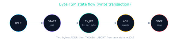
Byte FSM — START → 8 bits → ACK → STOP
The byte engine sequences one I2C frame: START condition, address byte (from CSR ADDR), data byte (from CSR TXDATA), ACK check, STOP. It issues single-bit commands to the bit engine and waits for bit_done.
// i2c_byte_fsm.v — byte-level I2C master sequencer
module i2c_byte_fsm (
  input  wire       clk,
  input  wire       rst_n,
  input  wire       start_pulse,
  input  wire       abort,
  input  wire [6:0] slave_addr,
  input  wire [7:0] txdata,
  output reg        busy,
  output reg        done,
  output reg        nack,
  output reg        cmd_valid,
  output reg [2:0]  cmd,
  output reg        bit_val,
  input  wire       bit_done,
  input  wire       ack_sda
);
  localparam ST_IDLE    = 4'd0;
  localparam ST_START   = 4'd1;
  localparam ST_TX_BIT  = 4'd2;
  localparam ST_TX_ACK  = 4'd3;
  localparam ST_STOP    = 4'd4;

  localparam CMD_START      = 3'd1;
  localparam CMD_STOP       = 3'd2;
  localparam CMD_DATA_BIT   = 3'd3;
  localparam CMD_SAMPLE_ACK = 3'd4;

  reg [3:0]  state;
  reg [7:0]  shifter;
  reg [2:0]  bit_cnt;   // 7 down to 0
  reg        second_byte; // 0=addr, 1=data

  always @(posedge clk or negedge rst_n) begin
    if (!rst_n) begin
      state <= ST_IDLE;
      busy <= 1'b0; done <= 1'b0; nack <= 1'b0;
      cmd_valid <= 1'b0; cmd <= 3'd0; bit_val <= 1'b0;
      shifter <= 8'h00; bit_cnt <= 3'd7; second_byte <= 1'b0;
    end else begin
      cmd_valid <= 1'b0;
      if (abort && state != ST_IDLE) begin
        state <= ST_IDLE; busy <= 1'b0; done <= 1'b0;
      end else case (state)
        ST_IDLE: begin
          done <= 1'b0; nack <= 1'b0;
          if (start_pulse) begin
            busy <= 1'b1;
            second_byte <= 1'b0;
            shifter <= {slave_addr, 1'b0};  // write addr byte = (addr<<1)|0
            bit_cnt <= 3'd7;
            state <= ST_START;
          end
        end
        ST_START: begin
          cmd_valid <= 1'b1; cmd <= CMD_START;
          if (bit_done) state <= ST_TX_BIT;
        end
        ST_TX_BIT: begin
          cmd_valid <= 1'b1;
          cmd <= CMD_DATA_BIT;
          bit_val <= shifter[7];
          if (bit_done) begin
            shifter <= {shifter[6:0], 1'b0};
            if (bit_cnt == 0)
              state <= ST_TX_ACK;
            else
              bit_cnt <= bit_cnt - 1'b1;
          end
        end
        ST_TX_ACK: begin
          cmd_valid <= 1'b1; cmd <= CMD_SAMPLE_ACK;
          if (bit_done) begin
            if (ack_sda) nack <= 1'b1;
            if (!second_byte) begin
              second_byte <= 1'b1;
              shifter <= txdata;
              bit_cnt <= 3'd7;
              state <= ST_TX_BIT;
            end else
              state <= ST_STOP;
          end
        end
        ST_STOP: begin
          cmd_valid <= 1'b1; cmd <= CMD_STOP;
          if (bit_done) begin
            busy <= 1'b0; done <= 1'b1;
            state <= ST_IDLE;
          end
        end
        default: state <= ST_IDLE;
      endcase
    end
  end
endmodule
Top wrapper — wiring it together
The top module instantiates CSR, byte FSM, and bit engine. Pad cells use open-drain modeling: when oe=0, the TB pull-up wins.
// i2c_master_top.v — CSR + byte FSM + bit engine
module i2c_master_top (
  input  wire        clk,
  input  wire        rst_n,
  input  wire        reg_wr,
  input  wire        reg_rd,
  input  wire [7:0]  reg_addr,
  input  wire [31:0] reg_wdata,
  output wire [31:0] reg_rdata,
  output wire        scl_out,
  output wire        scl_oe,
  output wire        sda_out,
  output wire        sda_oe,
  input  wire        sda_i,
  output wire        irq
);
  wire       ctrl_start, ctrl_abort, ctrl_irq_en;
  wire       stat_busy, stat_nack, stat_done;
  wire [6:0] reg_slave_addr;
  wire [7:0] reg_txdata, reg_rxdata;
  wire [15:0] reg_clkdiv;
  wire       cmd_valid, bit_done;
  wire [2:0] cmd;
  wire       bit_val, ack_sda;

  i2c_csr u_csr (
    .clk(clk), .rst_n(rst_n),
    .reg_wr(reg_wr), .reg_rd(reg_rd),
    .reg_addr(reg_addr), .reg_wdata(reg_wdata), .reg_rdata(reg_rdata),
    .ctrl_start(ctrl_start), .ctrl_abort(ctrl_abort), .ctrl_irq_en(ctrl_irq_en),
    .stat_busy(stat_busy), .stat_nack(stat_nack), .stat_done(stat_done),
    .reg_slave_addr(reg_slave_addr), .reg_txdata(reg_txdata),
    .reg_rxdata(reg_rxdata), .reg_clkdiv(reg_clkdiv)
  );

  i2c_byte_fsm u_byte (
    .clk(clk), .rst_n(rst_n),
    .start_pulse(ctrl_start), .abort(ctrl_abort),
    .slave_addr(reg_slave_addr), .txdata(reg_txdata),
    .busy(stat_busy), .done(stat_done), .nack(stat_nack),
    .cmd_valid(cmd_valid), .cmd(cmd), .bit_val(bit_val),
    .bit_done(bit_done), .ack_sda(ack_sda)
  );

  i2c_bit_engine u_bit (
    .clk(clk), .rst_n(rst_n), .clkdiv(reg_clkdiv),
    .cmd_valid(cmd_valid), .cmd(cmd), .bit_val(bit_val),
    .bit_done(bit_done), .ack_sda(ack_sda),
    .scl_out(scl_out), .scl_oe(scl_oe),
    .sda_out(sda_out), .sda_oe(sda_oe), .sda_i(sda_i)
  );

  assign reg_rxdata = 8'h00;  // placeholder for read path extension
  assign irq = ctrl_irq_en && (stat_done || stat_nack);
endmodule
Coding style notes
- Non-blocking assigns in all sequential always blocks —
<=only in FSM and counters - Sync reset or async assert / sync deassert — this design uses async assert on
rst_nfor simplicity; production blocks often sync deassert - Default outputs every cycle —
cmd_valid <= 0at top of always block prevents accidental multi-cycle commands - One-hot or enum states — 4-bit state encoding is fine at this scale; switch to
localparam+ case for lint clarity - No latches — every
casebranch assigns all regs; combinational CSR read in separatealways @(*) - Pulse signals — START is one cycle; don't leave it high or you'll restart mid-transaction
Synthesis note: pad oe signals map to IOBUF cells on FPGA/ASIC. The bit engine's clkdiv counter is your main timing path — keep it registered, not combinational.
This implementation omits clock stretching (SCL held low by slave). That's acceptable for the capstone — document it as a gap in your design review (11.6).
Implementation checklist
- CSR offsets match 11.2 spec (CTRL/STAT/ADDR/TXDATA/RXDATA/CLKDIV)
- ADDR holds 7-bit slave address; byte FSM forms
{addr,1'b0}write byte - START pulse kicks byte FSM only when not BUSY
- ABORT returns FSM to IDLE and clears BUSY
- Bit engine uses oe-based open-drain — no active-high SDA drive
- ACK sampled with SDA released (sda_oe=0)
- STAT.DONE sets after STOP completes; NACK sets if slave doesn't pull SDA low
- Top module wires all three sub-blocks with named ports
🎯 What to remember
- Three layers: CSR (software), byte FSM (protocol), bit engine (pads).
- Open-drain = drive 0 or release — never fight the pull-up.
- Byte FSM issues one bit command at a time; bit engine owns timing.
- Paste all four modules into the simulator — next lesson adds the self-checking TB (11.5).