I2C protocol crash course
Before you write a single line of RTL, you must speak the bus language. I2C (Inter-Integrated Circuit) is a two-wire, multi-drop serial protocol: one clock (SCL), one data (SDA), open-drain pads, and a strict sequence of START, address, data bytes, ACK/NACK, and STOP. This lesson gives you the protocol fluency every I2C master designer needs.
I2C is a master-driven, byte-oriented bus where the master generates SCL, both lines are open-drain with pull-ups, data is transferred MSB-first, and every 8-bit byte is followed by a 9th ACK bit driven by the receiver.
Two wires, many devices
I2C connects a master (your SoC controller) to one or more slaves (EEPROM, PMIC, sensor) on a shared bus. Only two signals leave the chip — dramatically fewer pins than SPI. The trade-off: shared bandwidth, pull-up limited speed, and protocol complexity.
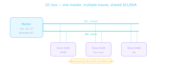
Every device connects SCL and SDA in parallel. Only the device driving low wins — wired-AND via open-drain.
| Role | Responsibility | Typical device |
|---|---|---|
| Master | Generates SCL, initiates START/STOP, sends address | SoC I2C controller, MCU |
| Slave | Responds when addressed; ACKs bytes; may clock-stretch | EEPROM, RTC, PMIC, sensor |
| Bus | Shared SCL + SDA with pull-up resistors | PCB traces + Rp (2.2k–10k typical) |
Analogy: I2C is a classroom where the teacher (master) calls roll by address. Only the student whose name is called may speak on SDA during the data phase — everyone else releases the line (high-Z) and listens.
Open-drain — why idle is high
Both SCL and SDA use open-drain (open-collector) pads: a device can only pull the line low or release it (high-Z). External pull-up resistors (Rp) pull the line to logic high when nobody drives low. This wired-AND property lets multiple devices share one wire without contention damage.
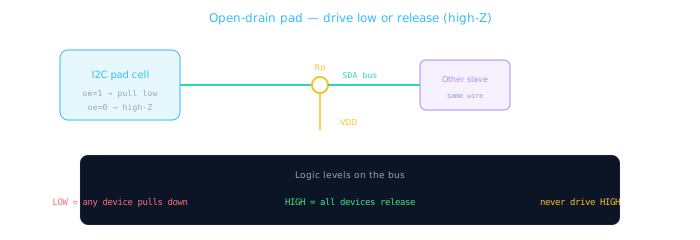
RTL implication: your pad logic is assign sda = oe ? 1'b0 : 1'bz; — never actively drive high.
Wired-AND
If any device pulls low, the bus reads low. Multiple masters and slaves can coexist safely.
Idle = high
When no transaction is active, both SCL and SDA float high via Rp. This is the bus idle state.
Rp trade-off
Smaller Rp → faster rise, more static current. Larger Rp → slower edges, limits max clock rate.
Modeling I2C with push-pull outputs in simulation "works" until you hit multi-master or clock-stretch scenarios. Always use open-drain + pull-up in TB pad models.
START and STOP conditions
START and STOP are signaling events, not data bytes. They frame every transaction and are the first things your waveform checker should assert.
| Condition | Rule | Meaning |
|---|---|---|
| START (S) | MUST SDA falls while SCL is high | Master claims the bus; a new transaction begins |
| STOP (P) | MUST SDA rises while SCL is high | Transaction ends; bus returns to idle |
| Repeated START (Sr) | SHOULD START without preceding STOP | Change direction or sub-address without releasing bus |
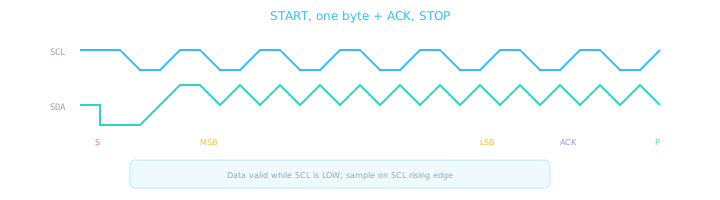
SDA may change only when SCL is low (except START/STOP). Receivers sample SDA on SCL rising edges.
A START followed immediately by STOP with no clock pulses is legal but useless. More common bug: changing SDA while SCL is high during a data byte — that creates a false START/STOP and corrupts the frame.
Byte transfer — MSB first, 9 clocks
Each byte takes 8 data bits + 1 ACK bit = 9 SCL pulses. Bits are transmitted MSB first (bit 7 down to bit 0). The master drives SCL for every bit; the data driver alternates between master and slave depending on transaction direction.
| Phase | SCL | SDA driver | Action |
|---|---|---|---|
| Setup | Low | Transmitter | Set next data bit on SDA |
| Sample | Rising edge | — | Receiver latches SDA bit |
| Hold | High | Transmitter holds | SDA stable while SCL high |
| ACK (9th) | 9th pulse | Receiver | Pull low = ACK, leave high = NACK |
ACK vs NACK: After the master sends an address or write byte, the slave ACKs by pulling SDA low on the 9th clock. After the master reads a byte, the master ACKs (more data coming) or NACKs (last byte, stop next). A missing ACK usually means wrong address or slave not ready.
7-bit addressing + R/W bit
Immediately after START, the master sends a 7-bit slave address followed by a 1-bit direction flag (R/W̅). Together this is the address frame — 8 bits total, MSB of the 7-bit address goes first.
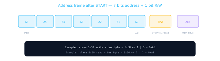
Software datasheets give 7-bit address (e.g. 0x50). Hardware shifts left and appends R/W.
Common transaction patterns:
- Write: START → addr+W → ACK → data byte(s) → ACK each → STOP
- Read: START → addr+R → ACK → master receives bytes → master ACK/NACK each → STOP
- Write-then-read: START → addr+W → reg addr → Sr → addr+R → read bytes → STOP
// Slave 0x50 (7-bit), internal reg 0x0010, read 2 bytes
// Phase 1: set pointer (write)
S  +  0xA0  +  ACK  +  0x00  +  ACK  +  0x10  +  ACK
// Phase 2: repeated START, read data
Sr +  0xA1  +  ACK  +  D0  +  ACK  +  D1  +  NACK  +  P
Read transactions — master drives final NACK
During a read, the slave drives data bits but the master drives ACK/NACK on the 9th bit of each byte. This is the most commonly inverted rule in student implementations.
| Byte position | Data driver | 9th bit driver | 9th bit value |
|---|---|---|---|
| Bytes 1 .. N-1 | Slave | Master | ACK (SDA low) — "send more" |
| Byte N (last) | Slave | Master | NACK (SDA high) — "I'm done" |
Why NACK the last byte? It signals the slave to stop driving. After NACK, the master generates STOP. Without NACK, the slave would prepare another byte the master does not want.
Speed modes and timing intuition
You do not need every number from the I2C spec memorized — but you need the relationships that drive RTL divider choices and pad timing constraints.
| Mode | Max fSCL | Intuition |
|---|---|---|
| Standard-mode | 100 kHz | Legacy sensors; generous setup/hold; slow Rp OK |
| Fast-mode | 400 kHz | Most common target for SoC masters |
| Fast-mode Plus | 1 MHz | Needs smaller Rp, shorter traces |
- tHD;STA: minimum LOW time on SCL after START before first clock — your FSM must hold SCL low long enough.
- tSU;STA: setup time for repeated START — SDA setup before SCL rises.
- tBUF: bus free time between STOP and next START — inter-transaction gap.
- Rise time: limited by Rp and bus capacitance Cb — large Cb means you cannot run 400 kHz with 10k pull-ups.
RTL takeaway: your clock divider sets target SCL period; your bit FSM must stretch LOW/HIGH phases to meet tLOW and tHIGH minimums. We'll architect this in Lesson 11.3 and size DIV per the 11.2 CSR map.
Repeated START — write-then-read without STOP
EEPROMs and sensors often need a register pointer write followed immediately by a read. Releasing the bus with STOP between phases risks another master stealing the bus or the slave losing its internal address pointer. Repeated START (Sr) solves this: issue a second START without an intervening STOP.
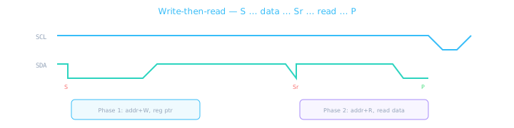
Sr looks like START electrically — SDA↓ while SCL high — but occurs mid-transaction without bus idle gap.
| Step | Bus byte | Direction | Notes |
|---|---|---|---|
| 1. START | — | — | Claim bus |
| 2. Address + W | (0x50<<1)|0 = 0xA0 | Master → slave | Slave ACKs if present |
| 3. Reg pointer | 0x10 (example) | Master → slave | Sets internal address |
| 4. Repeated START | — | — | Bus stays busy — no STOP |
| 5. Address + R | (0x50<<1)|1 = 0xA1 | Master → slave | Slave ACKs, prepares read |
| 6. Data byte(s) | D0, D1, … | Slave → master | Master NACKs last byte |
| 7. STOP | — | — | Release bus |
Using STOP then START instead of Sr works on a quiet bus but violates the spec intent and adds tBUF delay. Some slaves reset their pointer on STOP. Always use Sr for atomic write-then-read.
Multi-master awareness
Some buses have multiple masters (e.g. SoC + external tester). I2C handles this with arbitration: if two masters drive SDA differently during an address byte, the master reading '1' when it drove '0' loses and backs off. Clock stretching also interacts with multi-master — another reason open-drain modeling matters.
For this capstone, your I2C master IP is single-master. Know that multi-master exists, but do not over-engineer arbitration unless the spec demands it.
Timing parameters — intuition table
These numbers come from the I2C specification (NXP UM10204). You do not memorize every picosecond — but your RTL divider and FSM phases must respect the relationships.
| Symbol | Name | Fast-mode (400 kHz) | RTL impact |
|---|---|---|---|
| tLOW | SCL low period | ≥ 1.3 µs | PH_SETUP + PH_FALL must sum ≥ tLOW |
| tHIGH | SCL high period | ≥ 0.6 µs | PH_RISE + PH_HIGH ≥ tHIGH; stretch extends this |
| tSU;DAT | SDA setup before SCL↑ | ≥ 100 ns | Set SDA in PH_SETUP before PH_RISE |
| tHD;DAT | SDA hold after SCL↓ | ≥ 0 ns (0.9 µs legacy) | Keep SDA stable through PH_FALL |
| tBUF | Bus free between transactions | ≥ 1.3 µs | Idle gap after STOP before next START |
| tSP | Pulse width spikes suppressed | ≤ 50 ns | Pad filtering — usually analog concern |
// pclk = 50 MHz → T_clk = 20 ns
// Target Fast-mode: f_scl = 400 kHz → T_scl = 2500 ns
// 4 phases per bit → T_phase = 625 ns → DIV = 625/20 = 31.25 → 31
// Actual T_scl = 4 * 31 * 20 ns = 2480 ns → 403 kHz (within spec)

// Standard-mode 100 kHz: DIV = 2500/20 = 125
localparam DIV_100K = 125;
localparam DIV_400K = 31;
Rp and Cb
Rise time tr ≈ 0.8473 × Rp × Cb. Long traces + many slaves → slow edges → lower max frequency.
Stretch extends tHIGH
Slave stretch is legal and unlimited (within reason). Master PH_HIGH must wait — no timeout in bare spec, but your IP SHOULD add one.
Sim vs silicon
Ideal 0 ns edges in RTL sim pass easily. Annotate SDF or add artificial rise delay for confidence.
Beginner mistakes — learn these now
- 8-bit vs 7-bit address confusion: writing
0xA0to the ADDR register when the datasheet says0x50— store 7-bit, shift in hardware. - Forgetting the 9th bit: counting 8 clocks per byte and sampling ACK on the wrong edge.
- Push-pull SDA in TB: masks clock-stretch and multi-drive bugs until silicon.
- STOP after NACK on read: correct for last byte; wrong if you NACK an address — check slave power and wiring.
- SDA glitch while SCL high: creates spurious START — often a FSM ordering bug (change data before SCL falls).
- No bus-free after STOP: starting next transaction too fast violates tBUF.
Simulation passes with ideal wires but fails in lab because pull-ups are missing or too large. Always include Rp and pad capacitance in timing-aware sims for sign-off confidence.
Protocol literacy checklist
- Draw START and STOP from memory (SDA transition while SCL high)
- Explain why I2C pads are open-drain and idle high
- Count 9 SCL pulses per byte including ACK
- Convert 7-bit address 0xNN to write/read bus bytes
- Describe write-then-read with repeated START
- State who drives ACK after address vs after read data
- Name at least two timing parameters and what they constrain
- Explain why master NACKs the last byte of a read
- Draw write-then-read with Sr between phases
Self-check — protocol quiz
- Bus is idle (SCL=H, SDA=H). Master pulls SDA low, then SCL low. Is this START? Answer: yes — SDA fell while SCL was high.
- How many SCL pulses for one address byte including ACK? Answer: 9.
- Slave address 0x34, read transaction — what is the first byte on SDA? Answer: (0x34<<1)|1 = 0x69.
- Who drives SDA during the 9th bit of a write data byte? Answer: the slave (ACK/NACK).
- Can SDA change while SCL is high during a data bit? Answer: no — only during START, STOP, or Sr.
- What happens if no slave ACKs the address? Answer: SDA stays high (NACK); master should STOP and report error.
Score 6/6 before moving to Lesson 11.2. If you miss the R/W bit or 9th-clock questions, re-read Sections 4 and 5.
Quick reference card
| Topic | Rule |
|---|---|
| Idle bus | SCL=H, SDA=H (pull-ups) |
| START | SDA↓ while SCL=H |
| STOP | SDA↑ while SCL=H |
| Data bit order | MSB (bit 7) first |
| Bits per byte | 8 data + 1 ACK = 9 clocks |
| 7-bit addr 0xNN write | First byte = (NN << 1) | 0 |
| 7-bit addr 0xNN read | First byte = (NN << 1) | 1 |
| Write ACK driver | Slave pulls low on 9th bit |
| Read last-byte ACK | Master NACKs (SDA high) |
| Write-then-read | Use Sr, not STOP between phases |
| Clock stretch | Slave holds SCL low; master waits |
| Fast-mode | 400 kHz max; tLOW ≥ 1.3 µs |
🎯 What to remember
- I2C = open-drain SCL/SDA, pull-ups, wired-AND, idle high.
- START: SDA↓ with SCL high. STOP: SDA↑ with SCL high.
- Bytes are MSB-first; every byte has a 9th ACK bit from the receiver.
- Address frame = 7-bit addr + R/W bit; store 7-bit in registers, shift in logic.
- Repeated START enables write-then-read without releasing the bus.