Write the 1-page I2C master/slave spec
Great RTL starts on paper. Before architecture and Verilog, you need a one-page micro-spec that answers: what does this block do, how does software talk to it, what must it guarantee on the bus, and how do we know it works? This lesson walks you through a complete master-focused spec — the same document you'll refine as your capstone deliverable.
A one-page spec is not vague — it is compressed clarity. Every sentence is either a requirement, an interface definition, or a testable acceptance criterion. If you cannot test it, it does not belong in MUST.
Why spec before RTL
Jumping straight into Verilog produces a block that "sort of works" in one testbench but breaks on the second slave, the wrong clock rate, or a missing NACK path. A micro-spec forces you to decide:
- What transactions the master supports (write, read, write-then-read)
- How firmware kicks off a transfer and polls completion
- What happens on NACK, bus error, and timeout
- What you are explicitly not building (non-goals)
Analogy: The spec is a restaurant menu with prices and allergens. Architecture is the kitchen layout. RTL is cooking. You would not build a kitchen without knowing whether you serve steak or sushi.
Block diagram — master IP context
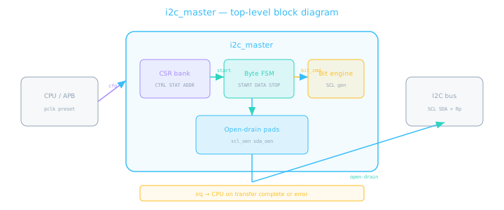
Software sees CSRs. The bus sees open-drain SCL/SDA. Internal FSM + bit engine bridge the two worlds.
Complete reference micro-spec
Below is the golden one-pager for this capstone. Copy it into your notebook and annotate decisions you would change for your project.
1. Purpose
i2c_master is a single-master I2C controller that lets firmware initiate write, read, and write-then-read (repeated START) transactions on a shared open-drain bus at Standard-mode (100 kHz) or Fast-mode (400 kHz), selectable via clock divider.
2. Scope — non-goals
- NOT a slave controller; NOT multi-master arbitration
- NOT 10-bit addressing; NOT HS-mode (3.4 MHz)
- NOT DMA — CPU loads TX/RX FIFO registers directly
- MAY add SMBus alert later; out of scope for v1
3. External interfaces
| Interface | Signals | Notes |
|---|---|---|
| CPU (APB) | pclk, preset_n, psel, penable, pwrite, paddr[7:0], pwdata[31:0], prdata[31:0], pready | 32-bit aligned CSRs; always ready in 1 cycle |
| I2C pads | scl_i, scl_o, scl_oen_n, sda_i, sda_o, sda_oen_n | Open-drain: oen_n=0 drives low, oen_n=1 releases |
| Interrupt | irq | Level-high while STAT.done or STAT.err set and unmasked |
4. CSR map
| Offset | Name | Access | Description |
|---|---|---|---|
| 0x00 | CTRL | RW | [0] EN enable; [1] START auto-clear; [2] RD 1=read 0=write; [3] STOPIE stop-on-NACK |
| 0x04 | STAT | RO | [0] BUSY; [1] DONE W1C; [2] NACK W1C; [3] ARB_LOST tie 0 |
| 0x08 | ADDR | RW | [6:0] 7-bit slave address (not shifted) |
| 0x0C | TX | WO | Next write byte or register pointer for write-then-read |
| 0x10 | RX | RO | Last received byte after read completes |
| 0x14 | DIV | RW | [15:0] half-period counts in pclk cycles; fSCL ≈ pclk / (4 × DIV) |
| 0x18 | BCNT | RW | [7:0] bytes to xfer in read or multi-byte write (1–16) |
5. Requirements
MUST Generate legal START, STOP, and repeated START per I2C spec.
MUST Transmit address as (ADDR << 1) | RD with MSB first.
MUST Sample SDA on SCL rising edge; change SDA only when SCL is low (except START/STOP).
MUST Set STAT.NACK if slave does not ACK address or write byte.
MUST Support clock stretching: hold SCL low until scl_i reads high.
SHOULD Abort transaction and release bus if SCL held low > 25 ms (timeout).
SHOULD Insert tBUF bus-free time (≥ 2 SCL periods) after STOP before next START.
MAY Implement 16-byte FIFO in v2; v1 is single-byte TX/RX.
6. Firmware sequence — write 1 byte
- Write ADDR, TX, BCNT=1, DIV
- Write CTRL = EN | START (RD=0)
- Poll STAT.BUSY or wait for irq
- Check STAT.NACK; clear DONE
Spec writing workshop — bad vs good MUST
Vague requirements cause rework. Compare these pairs — the good version is observable and testable.
"The I2C block shall work correctly with all slaves."
"On address byte NACK, the master SHALL release SDA, generate STOP within 1 byte time, and set STAT.NACK within 2 pclk cycles."
"Support fast I2C."
"With DIV configured for 400 kHz at pclk=50 MHz, measured SCL period SHALL be 2500 ns ±5% in simulation."
"Handle errors gracefully."
"If STOPIE=1 and any byte receives NACK, the master SHALL abort remaining bytes and assert STAT.NACK."
Mixing implementation ("use a 4-state FSM") into requirements. The spec says what; architecture says how. Exception: pad interface style (open-drain oen) is a requirement because it affects the PCB.
Acceptance tests A1–A6
Every MUST maps to at least one acceptance test. These become your directed testbench scenarios in Module 11 verification.
| ID | Scenario | Pass criteria |
|---|---|---|
| A1 | Single-byte write to slave 0x50, data 0xAB | Bus shows S, 0xA0, ACK, 0xAB, ACK, P; STAT.DONE=1, NACK=0 |
| A2 | Single-byte read from slave 0x50 | Bus shows S, 0xA1, ACK, data byte, master NACK, P; RX=slave data |
| A3 | Write-then-read: set reg 0x10, read 2 bytes | Sr between phases; correct addr bytes 0xA0 then 0xA1; RX holds last byte |
| A4 | Address NACK (no slave at 0x77) | STAT.NACK=1; STOP on bus; BUSY clears; no hang |
| A5 | Clock stretch: slave holds SCL low 5 µs mid-byte | Master waits; transaction completes; no premature sampling |
| A6 | DIV sweep: 100 kHz and 400 kHz | Measured SCL period within ±5% of target at both settings |
// A1: directed write check (pseudo-code)
task test_a1_write_byte;
  cfg_slave(7'h50, resp='{ack_addr:1, ack_data:1});
  fw_write(ADDR, 7'h50);
  fw_write(TX,   8'hAB);
  fw_write(BCNT, 8'd1);
  fw_write(CTRL, EN | START);
  wait_done();
  assert(stat.nack == 0) else $error("A1: unexpected NACK");
  assert(bus_log == '{S, 8'hA0, ACK, 8'hAB, ACK, P})
    else $error("A1: bus sequence mismatch");
endtask
MUST / SHOULD / MAY reference
| Keyword | Meaning | Verification |
|---|---|---|
| MUST | Mandatory — violation is a defect | Blocking acceptance test; fails sign-off |
| SHOULD | Strongly recommended; waiver needs doc | Test exists; failure is bug or approved exception |
| MAY | Optional enhancement | No test required unless implemented |
Traceability
Each MUST links to an acceptance test ID. Reviewers can audit coverage in one table.
Non-goals
Explicitly listing what you won't build prevents scope creep and false expectations.
Testable
If you cannot write A7 for a sentence, rewrite the sentence until you can.
Traceability matrix — MUST to test
Professional specs include a traceability table linking every MUST to an acceptance test and a verification method. This is what sign-off reviewers ask for first.
| Req ID | MUST statement | Test | Method |
|---|---|---|---|
| R-01 | Legal START/STOP generation | A1, A2 | Bus monitor SVA |
| R-02 | 7-bit addr shifted with R/W | A1, A3 | Waveform compare |
| R-03 | STAT.NACK on missing slave | A4 | Directed + self-check |
| R-04 | Clock stretch wait | A5 | TB holds scl_i low |
| R-05 | DIV sets f_scl ±5% | A6 | $time measurement |
| R-06 | Repeated START for w-t-r | A3 | Bus log sequence |
| R-07 | Open-drain oen_n interface | lint + A1 | Pad cell review |
| R-08 | irq on done | nack | A1, A4 | IRQ pin assert |
Req ID
Number every requirement R-01, R-02… Changes in ECOs reference IDs, not paragraph text.
Coverage
If a MUST has no test row, it is not a requirement — it is a wish.
Sign-off
PM signs when all A-tests pass and traceability matrix is 100% filled.
Firmware cookbook — three recipes
The spec is not complete until firmware engineers can use it without asking you questions. Document these three sequences verbatim.
#define I2C_BASE  0x40008000
#define CTRL  (I2C_BASE + 0x00)
#define STAT  (I2C_BASE + 0x04)
#define ADDR  (I2C_BASE + 0x08)
#define TX    (I2C_BASE + 0x0C)
#define RX    (I2C_BASE + 0x10)
#define DIV   (I2C_BASE + 0x14)
#define BCNT  (I2C_BASE + 0x18)

// Recipe 1: write 1 byte to slave
void i2c_write_byte(uint8_t slave7, uint8_t data) {
  writel(slave7, ADDR);
  writel(data, TX);
  writel(1, BCNT);
  writel(EN | START, CTRL);       // RD=0 implied
  while (readl(STAT) & BUSY);
  if (readl(STAT) & NACK) handle_nack();
  writel(DONE | NACK, STAT);      // W1C clear
}

// Recipe 2: read N bytes
uint8_t i2c_read_bytes(uint8_t slave7, int n) {
  writel(slave7, ADDR);
  writel(n, BCNT);
  writel(EN | START | RD, CTRL);
  while (readl(STAT) & BUSY);
  return (uint8_t)readl(RX);    // last byte in v1 single-RX
}

// Recipe 3: write-then-read (set reg ptr, read 1 byte)
uint8_t i2c_reg_read(uint8_t slave7, uint16_t reg, int n) {
  writel(slave7, ADDR);
  writel(reg >> 8, TX); writel(reg & 0xFF, TX);  // v2: multi-TX
  writel(EN | START | REP_START_EN, CTRL);       // FSM handles Sr
  // ... poll, read RX
}
| Recipe | CTRL bits | BCNT | Expected STAT |
|---|---|---|---|
| Write 1 byte | EN | START | 1 | DONE=1, NACK=0 |
| Read N bytes | EN | START | RD | N | DONE=1 after last NACK sent |
| Write-then-read | EN | START (FSM does Sr) | ptr + read count | DONE=1; RX holds last byte |
Timing budget — from pclk to bus
The DIV register is not arbitrary — tie it to a formula in the spec so integrators can configure any supported pclk without your help.
- MUST Document:
DIV = floor(pclk / (4 × f_target)) - SHOULD Provide a lookup table for common pclks: 25, 50, 100 MHz
- MAY Auto-compute DIV from a CFG.FMODE bit (100k/400k enum)
Integration note: if pclk can change (DVFS), software must reprogram DIV or pause I2C during clock switch. Document this in the spec assumptions section.
Your deliverable — fill-in template
Complete this template for your capstone variant. Bring it to architecture (11.3) and RTL (11.4).
# i2c_master — 1-page spec (YOUR NAME / DATE)

## Purpose
[One paragraph: what, which modes, master/slave]

## Non-goals
- [ ] ...
- [ ] ...

## Interfaces
| Interface | Signals | Notes |
|-----------|---------|-------|
| CPU       |         |       |
| I2C pads  |         |       |
| irq       |         |       |

## CSR map
| Offset | Name | Access | Bit fields |
|--------|------|--------|------------|
| 0x00   | CTRL | RW     |            |
| ...    |      |        |            |

## MUST requirements (min 8)
1. ...
2. ...

## SHOULD requirements (min 2)
1. ...

## Acceptance tests
| ID | Scenario | Pass criteria |
|----|----------|---------------|
| A1 |          |               |
| ...|          |               |

## Firmware cookbook
Write 1 byte: ...
Read N bytes: ...
Write-then-read: ...
Spec review checklist
- Purpose states master vs slave and supported transaction types
- Non-goals explicitly exclude at least 3 out-of-scope features
- CSR map covers CTRL, STAT, ADDR, TX, RX, DIV with bit fields
- 7-bit address stored unshifted; shift documented in MUST
- Every MUST is testable — mapped to A1–An acceptance test
- Open-drain pad interface documented (oen polarity!)
- Clock stretch and NACK behavior specified (no "hang forever")
- Firmware sequence written for write, read, and write-then-read
- Traceability matrix links every MUST to an acceptance test
Top-level port list — integration reference
Architects and PD engineers need the exact port list before floorplanning. Copy this into your spec appendix.
module i2c_master (
  // Clock / reset
  input  wire        pclk,
  input  wire        preset_n,
  // APB config
  input  wire        psel,
  input  wire        penable,
  input  wire        pwrite,
  input  wire [7:0]  paddr,
  input  wire [31:0] pwdata,
  output wire [31:0] prdata,
  output wire        pready,
  // I2C pads (open-drain)
  input  wire        scl_i,
  output wire        scl_o,
  output wire        scl_oen_n,
  input  wire        sda_i,
  output wire        sda_o,
  output wire        sda_oen_n,
  // Interrupt
  output wire        irq
);
| Port | Width | Direction | Description |
|---|---|---|---|
pclk | 1 | in | APB clock; also bit engine clock in v1 |
scl_oen_n | 1 | out | 0=drive SCL low; 1=release (open-drain) |
sda_oen_n | 1 | out | 0=drive SDA low; 1=release |
irq | 1 | out | Level-high interrupt; clear via STAT W1C |
Deliverable checkpoint: your completed spec template + this port list + traceability matrix = sign-off package for architecture review (11.3). Bring all three before writing RTL in Lesson 11.4.
🎯 What to remember
- Spec before RTL — compressed clarity, not vague wishes.
- CSR map + pad interface + irq are the three external contracts.
- MUST = testable; link each to acceptance test A1–A6.
- Non-goals prevent scope creep (no multi-master, no 10-bit in v1).
- Bad specs say "work correctly"; good specs say what happens on NACK in nanoseconds.