Design review pack — lint, CDC, timing, area
Shipping RTL means defending it in review. This lesson is your close-out checklist: what to run before you call the I2C capstone done, how to document decisions honestly, and a one-page write-up template you can submit or bring to an interview.
Reviewers don't ask "does it simulate?" — they ask "will it fail in silicon?" Lint, CDC, and timing thinking catch the failures simulation hides. Document what you checked and what you knowingly deferred.
Review funnel — before you sign off
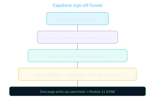
Simulation proves functional intent. Lint/CDC/timing prove synthesizability and robustness.
Lint checklist — I2C-specific
Run your linter (or eyeball with this list) on all synthesizable modules from Lesson 11.4. Fix or document every item.
- No latches — every
always @(posedge clk)assigns all regs in all branches; CSR read in separatealways @(*) - No multi-drive on oe — only bit engine drives
sda_oe/scl_oe; no combinational assign fighting the pad cell - No incomplete case — byte FSM
default → IDLE; bit enginedefault → CMD_IDLE - Async reset discipline — if using
negedge rst_n, document sync deassert plan for ASIC; FPGA often accepts async assert - No blocking in sequential logic —
=only in testbench and combinational blocks - Width mismatches —
bit_cntis 3 bits for 0–7;clkdivis 16 bits, compared to 16-bit counter - Unused inputs — tie off or document
reg_rxdataplaceholder - X propagation — sim shows no X on
sda_iafter reset (bus model has pull-up)
assign sda = sda_out; without tristate — linter flags multi-driver when slave model also connects. Production fix: IOBUF with T pin tied to !sda_oe.
// Synthesis-friendly pad interface (FPGA IOBUF or ASIC pad macro)
module i2c_pad_io (
  input  wire pad_in,     // from pin
  input  wire core_out,   // 0 = drive low
  input  wire core_oe,    // 1 = actively drive (open-drain: only drive 0)
  output wire pad_out     // to core (sampled input)
);
  // Behavioral model for sim; replace with IOBUF in FPGA flow
  assign pad_out = pad_in;
  // pad pin resolved externally: oe=0 → release (pull-up)
endmodule
CDC and open-drain notes
I2C is a slow serial protocol, but pad sampling still crosses clock domains in the strict sense — sda_i changes asynchronously to clk.
| Signal | Domain | Risk | Mitigation |
|---|---|---|---|
sda_i (pad input) | Async → sys_clk | Metastability on ACK sample | 2-flop synchronizer OR sample only when SCL stable high (our design) |
ctrl_start | CSR → byte FSM | Glitch if pulse too narrow | Single-cycle pulse in same clock domain — OK |
irq | sys_clk → CPU | If CPU is different clock | Level IRQ + sync in SoC — document as integration task |
| Open-drain bus | Analog/time | Rise time, bus capacitance | Pull-up resistor sizing — board-level, note in review |
Interview answer: "SDA is sampled synchronously while SCL is high in the bit engine — we only sample when the protocol guarantees setup time. For production ASIC I'd add a 2-FF sync on sda_i or use a dedicated IO cell with Schmitt input."
This capstone does not implement a full synchronizer on sda_i — that's a documented gap. Say so in your write-up; reviewers respect honesty over hand-waving.
Timing and area intuition
Critical path
clkdiv counter decrement → compare to zero → next-state in bit engine. At 100 MHz sys_clk with clkdiv=50, I2C ~1 MHz — plenty of margin.
Area estimate
~200–400 flops: CSR (6 regs), byte FSM (state + shifter), bit engine (counter + phase). Tiny vs a CPU or DSP block.
Clock gating opportunity
Gate clk to bit engine when byte FSM is IDLE. CSR stays awake for software access. Easy power win in ASIC flows.
The bit engine's cnt register runs every cycle during a transaction — that's intentional (bit-banged timing). Don't try to pipeline it; I2C is inherently sequential.
One-page design review template
Copy this structure. Fill in each section — one paragraph max per heading. Submit as PDF or markdown.
1. Design summary
I2C master with CSR map (CTRL/STAT/ADDR/TXDATA/RXDATA/CLKDIV), byte FSM for write transactions, bit engine with open-drain pad drivers. Verified with self-checking TB: write+ACK, NACK, abort.
2. Block diagram reference
Three layers: i2c_csr → i2c_byte_fsm → i2c_bit_engine. Software polls STAT.DONE. IRQ optional on completion.
3. Lint results
Ran [tool/manual review]. Fixed: [list]. Waived: [list with reason]. No latches, no multi-drive on oe.
4. CDC / pad sampling
sda_i sampled when SCL high in bit engine. Acknowledged gap: no 2-FF sync — acceptable at teaching clock rates; would add for tape-out.
5. Timing / performance
CLKDIV=50 @ 100 MHz → ~1 MHz I2C. Critical path in clkdiv counter. Meets timing in [FPGA/estimated].
6. Known limitations (honest gaps)
No clock stretching. Single-byte write only. No 10-bit addressing. No read path populated. No multi-master arbitration.
7. Verification summary
3 directed tests, all PASS. Waveform spot-check on TEST 1 confirms START/addr/data/ACK/STOP.
8. Sign-off
Designer: [name] · Date: [date] · Ready for integration: Y/N
# I2C Master — Design Review (Module 11 Capstone)

## Summary
[One sentence: what the block does and bus role]

## Architecture
- CSR: CTRL(START/ABORT/IRQ_EN), STAT(BUSY/NACK/DONE), ADDR, TXDATA, CLKDIV
- Byte FSM: START → addr byte → data byte → STOP
- Bit engine: open-drain scl/sda with oe, programmable clkdiv

## Lint
- [ ] No latches in FSM/CSR
- [ ] No multi-drive on pad oe
- [ ] Default cases in all FSMs
- Issues found: ___
- Issues fixed/waived: ___

## CDC / Pads
- sda_i sampling strategy: ___
- Known gap: ___

## Timing
- sys_clk: ___ MHz, CLKDIV: ___, effective I2C: ___ kHz
- Critical path: ___

## Verification
- TB: i2c_master_tb — tests: write+ACK, NACK, abort
- Result: ___ PASS / ___ FAIL

## Known gaps (extensions)
- Clock stretching, multi-byte, 10-bit addr, read path, multi-master

## Sign-off
Designer: ___  Date: ___  Status: ___
Module 11 checkpoint — what "done" means
You have finished Module 11 when all of the following are true:
- Four synthesizable RTL files simulate a write transaction (CSR, byte FSM, bit engine, top)
- CSR map matches Lesson 11.2 offsets and bit definitions
- Self-checking TB prints
=== ALL I2C TESTS PASSED ===— see 11.5 - You can explain START/ACK/STOP on a waveform without looking at the code
- One-page design review submitted (template above) with honest gaps listed
- You can answer "why open-drain?" and "what happens on NACK?" in an interview
Portfolio tip: Export one clean waveform screenshot (TEST 1) and attach it to your review doc. Interviewers love "here's the bus doing the right thing" more than 200 lines of unexplained Verilog.
Honest gaps — extensions you didn't build
Saying "it's done" without listing gaps is a red flag in review. Document these as future work:
| Gap | Why it matters | Extension path |
|---|---|---|
| Clock stretching | Slow slaves hold SCL low | Sample SCL input; pause counter when low |
| Multi-byte burst | EEPROM writes need >1 byte | CSR byte count + repeated TX without STOP |
| 10-bit addressing | Some sensors use it | Two address bytes after START |
| Read path | Half-duplex read | Shift in on TX_BIT, load RXDATA |
| Multi-master | Bus arbitration | Check SDA high before START; clock sync |
| SDA synchronizer | Metastability | 2-FF sync before ACK sample |
In interviews, lead with what you built and verified, then list two extensions you'd add first. "Clock stretching and read path" is a credible answer.
Pre-review self-audit — score yourself
Before submitting your write-up, walk this table. Score 0 = not done, 1 = partial, 2 = solid. Target ≥14/18.
| # | Question | Score (0–2) |
|---|---|---|
| 1 | Can you draw the three-layer block diagram from memory? | |
| 2 | Does CSR CTRL.START auto-clear after accept? | |
| 3 | Does ABORT return FSM to IDLE within a few cycles? | |
| 4 | Is sda_oe=0 during ACK sample (master releases)? | |
| 5 | Does STAT.NACK set when slave doesn't pull SDA low? | |
| 6 | TB test 1: slave captured correct data byte? | |
| 7 | TB test 2: NACK detected on wrong address? | |
| 8 | TB test 3: ABORT clears BUSY? | |
| 9 | Any latches reported by lint or manual review? | |
| 10 | Documented sda_i sampling / CDC approach? | |
| 11 | Listed ≥3 honest gaps with extension plan? | |
| 12 | Can you explain open-drain in one sentence? | |
| 13 | Waveform screenshot attached to review doc? | |
| 14 | CLKDIV math documented (sys_clk → I2C rate)? | |
| 15 | All code blocks use non-blocking in sequential logic? | |
| 16 | Default case in every FSM always block? | |
| 17 | IRQ behavior documented (level vs pulse)? | |
| 18 | Ready to defend in a 10-minute design review? |
Scoring: 16–18 = ship it. 12–15 = fix gaps before review. Below 12 = revisit Lessons 11.4–11.5, re-run TB, then return here.
Interview flash cards — defend your capstone
Module 12 goes deeper; use these now to rehearse out loud.
"Walk me through a write."
SW writes ADDR+TXDATA, pulses START. Byte FSM does START, addr byte, ACK check, data byte, ACK, STOP. Bit engine toggles SCL/SDA. STAT.DONE when finished.
"Why open-drain?"
Multiple devices share one wire. Anyone can pull low; no one drives high — pull-up resistor sets idle high. Prevents bus contention.
"What on NACK?"
Slave didn't ACK — STAT.NACK sets. Software decides retry or abort. We still complete STOP in this design to release the bus.
"Biggest risk in silicon?"
Pad sampling without sync; missing clock stretch for slow slaves; insufficient pull-up on long PCB traces. All documented in review gaps.
I built a synthesizable I2C master in three layers: CSR for software,
byte FSM for protocol sequencing, and a bit engine that drives open-drain
SCL/SDA with output-enable pads. Verified with a self-checking testbench
covering write-with-ACK, NACK detection, and abort. Documented lint/CDC/timing
in a one-page review. Known gaps: clock stretching, read path, and SDA
synchronizer — I'd add stretch detection first for real silicon.
Synthesis and constraints notes
When you move from sim to FPGA/ASIC, add these to your review appendix.
- Clock constraint:
create_clock -period 10 [get_ports clk]for 100 MHz sys_clk - False path:
sda_ito ACK flop may needset_false_pathor multicycle if you add synchronizer - IO standard: SCL/SDA pads → LVCMOS33 with open-drain IOBUF on Xilinx; bidir with
Tpin - Reset: If async assert, add
set_false_path -from [get_ports rst_n]or sync deassert cell - Don't optimize away: Keep pad
oeoutputs — synthesis must not merge them with internal logic
# I2C master — example timing constraints (adapt to your flow)
create_clock -name sys_clk -period 10.000 [get_ports clk]

# Async reset assert — adjust per your reset strategy
set_false_path -from [get_ports rst_n] -to [all_registers]

# Pad input — if using 2-FF sync, constrain sync chain instead
# set_input_delay -clock sys_clk -max 2.0 [get_ports sda_i]

# Generated I2C is slow — multicycle on bit engine counter path optional
# set_multicycle_path -setup 2 -from [get_cells u_bit/cnt*]
Don't pipeline the bit engine for "better timing" — you'll break I2C bit timing. If clkdiv path fails, register the compare result one cycle earlier, not add pipeline stages mid-bit.
Register and flop budget — area breakdown
Interviewers sometimes ask "how big is it?" Here's a reasonable flop estimate for your capstone — count them in your RTL if you want exact numbers.
| Module | Registers | Notes |
|---|---|---|
i2c_csr | ~80 flops | 6×32-bit shadow regs + control pulses |
i2c_byte_fsm | ~20 flops | state(4) + shifter(8) + bit_cnt(3) + flags |
i2c_bit_engine | ~25 flops | cnt(16) + phase + cmd + scl/sda/oe |
i2c_master_top | 0 | Wire-only hierarchy |
| Total | ~125 flops | Trivial vs 32-bit RISC core (5k–15k flops) |
Combinational logic is mostly muxes in CSR read and FSM next-state. Expect <500 LUTs on a small FPGA — dominated by the 16-bit counter compare, not the protocol logic.
- Power: Bit engine counter toggles every cycle during BUSY — clock-gate it when idle for ASIC.
- Floorplan: Pad ring placement for SCL/SDA near IO pins; CSR bus can be far from pads.
- DFT: Scan-insert FSM states; keep pad oe controllable in test mode for loopback.
Preview — Module 12: Career & Interview
Module 11 gave you a portfolio block. Module 12 turns it into interview ammunition:
- Resume bullet craft — how to describe the I2C capstone in one line recruiters understand
- Whiteboard FSM questions — draw byte FSM from memory; explain ACK timing
- Protocol follow-ups — "What if the slave NACKs?" "How would you add clock stretching?"
- RTL review role-play — present your design review doc as if to a senior engineer
- Job map — RTL designer vs verification vs FPGA — where this course points you
Bring your Module 11 write-up and waveform to Module 12. You'll practice defending it out loud — that's the skill that converts learning into offers.
How teams actually run RTL review
In industry, your one-page doc becomes a 30-minute meeting. Typical agenda:
- Author presents block diagram (5 min) — three layers, CSR map, bus role
- Walk one happy-path transaction (5 min) — waveforms or live sim
- Reviewer challenges (15 min) — "what on NACK?", "CDC on sda_i?", "stretch?"
- Action items (5 min) — fix, waive with rationale, or defer to v2
Your Module 11 write-up is practice for step 3. List gaps before the reviewer finds them — it signals maturity.
- Bring sim log showing
ALL I2C TESTS PASSED - Bring lint summary (even if "manual review — 0 issues")
- Bring waveform PNG of TEST 1 with START/ACK/STOP labeled
- Bring list of 3 extensions you'd implement next
Extension roadmap — phased v2 plan
Turn the gaps table into a credible roadmap. Interviewers respect phased delivery over "I'd add everything."
| Phase | Feature | Effort | Depends on |
|---|---|---|---|
| v1.1 | Clock stretching (sample scl_i, freeze PH_HIGH) | ~2 days | Bit engine only — see 11.3 PH_HIGH |
| v1.2 | Read path + master ACK/NACK on 9th bit | ~3 days | Byte FSM rd_phase; populate RXDATA CSR |
| v1.3 | Multi-byte burst via BCNT register | ~2 days | 11.2 BCNT + byte counter in FSM |
| v2.0 | Write-then-read (Sr), 10-bit addr, SDA 2-FF sync | ~1–2 weeks | Full regression; pad CDC for tape-out |
Portfolio tip: Pick v1.1 + v1.2 as your "next sprint" in the review doc — concrete and achievable in a weekend lab.
Interview Q&A — deep follow-ups
Beyond the flash cards in Section 9 — rehearse these with full answers.
| Question | Strong answer sketch |
|---|---|
| How do you form the address byte from software? | Store 7-bit in ADDR[6:0]; hardware sends (addr<<1)|RD MSB-first — per 11.2. |
| Who drives SDA during the 9th bit of a write? | Slave ACKs by pulling low; master releases (sda_oe=0) before sampling. |
What's your CDC story on sda_i? | Sample in PH_HIGH when SCL stable; acknowledge gap — add 2-FF sync for ASIC (documented in review). |
| How did you verify NACK? | Directed TB test 2 — wrong 7-bit addr, expect STAT.NACK — see 11.5. |
| Critical timing path? | clkdiv counter compare → phase advance; slow I2C so margin is large at 100 MHz. |
| What would you fix first for silicon? | Clock stretch + SDA synchronizer — highest risk on real slaves and async pads. |
Sample manager review comments
Real review feedback on student I2C masters — study these before your own review meeting.
"ADDR stores the shifted byte 0xA0 but your spec says 7-bit unshifted. Fix CSR or update spec — they're out of sync." → Align with 11.2: store 0x50, shift in RTL.
"Waveform shows SCL still high after START — you never pulled SCL low before the first data bit. Illegal per spec." → Bit engine START must end with SCL low.
"You sample sda_i combinatorially. Acceptable for FPGA lab clock rates — document as waiver with 2-FF sync planned for v2." → Don't hand-wave; cite review Section 3.
"Three directed tests are fine for capstone. Add one assertion on START condition before claiming 'protocol verified'." → Optional SVA: sda falls while scl high at transaction start.
"Approved for FPGA integration. Waive clock stretch and read path for v1 — tracked in roadmap v1.1/v1.2." → This is what a clean sign-off with honest gaps looks like.
🎯 What to remember
- Sim PASS is necessary but not sufficient — lint, CDC, timing thinking close the loop.
- Document honest gaps: stretch, multi-byte, 10-bit, read path.
- Submit the one-page review template — it's your capstone artifact.
- Module 12 turns this block into interview-ready stories.